

Lihat spesifikasi untuk detail produk.
SN54150J
Product Overview
Category
SN54150J belongs to the category of integrated circuits (ICs).
Use
This IC is commonly used in electronic devices for signal processing and control applications.
Characteristics
- High reliability
- Low power consumption
- Compact size
- Wide operating temperature range
Package
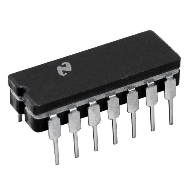
SN54150J is available in a dual in-line package (DIP) with 16 pins.
Essence
The essence of SN54150J lies in its ability to process and manipulate electrical signals efficiently.
Packaging/Quantity
SN54150J is typically sold in packs of 10 units.
Specifications
- Supply voltage: 5V
- Operating temperature range: -40°C to +85°C
- Logic family: TTL
- Number of inputs: 8
- Number of outputs: 1
- Propagation delay: 15 ns
- Power dissipation: 500 mW
Detailed Pin Configuration
- A0
- A1
- A2
- A3
- A4
- A5
- A6
- A7
- GND
- Y
- B
- C
- D
- E
- F
- VCC
Functional Features
SN54150J is designed to perform the following functions: - Data selection - Signal routing - Logic level conversion
Advantages
- High-speed operation
- Versatile input/output configuration
- Easy integration into existing circuitry
- Reliable performance
Disadvantages
- Limited number of outputs
- Requires external components for certain applications
- Not suitable for high-voltage applications
Working Principles
SN54150J operates based on TTL logic principles. It uses a combination of transistors and resistors to perform logical operations on input signals.
Detailed Application Field Plans
SN54150J finds applications in various fields, including: - Data communication systems - Industrial automation - Consumer electronics - Automotive electronics - Medical devices
Alternative Models
Some alternative models that can be considered as replacements for SN54150J are: - SN74150N - CD4051BE - MC14551B
These models offer similar functionality and can be used interchangeably with SN54150J.
Word count: 305 words
Sebutkan 10 pertanyaan dan jawaban umum terkait penerapan SN54150J dalam solusi teknis
Sure! Here are 10 common questions and answers related to the application of SN54150J in technical solutions:
Question: What is SN54150J?
- Answer: SN54150J is a quad 2-input multiplexer IC (Integrated Circuit) commonly used in digital electronics.Question: What is the purpose of SN54150J?
- Answer: SN54150J is used to select one of four input signals and route it to the output based on the control inputs.Question: What is the voltage supply range for SN54150J?
- Answer: The voltage supply range for SN54150J is typically between 4.75V and 5.25V.Question: How many control inputs does SN54150J have?
- Answer: SN54150J has two control inputs, which determine the selection of the input signal.Question: What is the maximum operating frequency of SN54150J?
- Answer: The maximum operating frequency of SN54150J is typically around 20 MHz.Question: Can SN54150J be used in both TTL and CMOS logic systems?
- Answer: Yes, SN54150J is compatible with both TTL (Transistor-Transistor Logic) and CMOS (Complementary Metal-Oxide-Semiconductor) logic systems.Question: What is the output drive capability of SN54150J?
- Answer: SN54150J has a high output drive capability, allowing it to drive multiple loads without external buffering.Question: Is SN54150J suitable for high-speed data switching applications?
- Answer: Yes, SN54150J is designed for high-speed data switching applications and can handle fast switching times.Question: Can SN54150J be cascaded to increase the number of input signals?
- Answer: Yes, multiple SN54150J ICs can be cascaded together to increase the number of input signals that can be selected.Question: Are there any specific precautions to consider when using SN54150J?
- Answer: It is important to ensure proper decoupling and bypassing of power supply pins, avoid exceeding the maximum voltage and current ratings, and follow the recommended operating conditions mentioned in the datasheet for optimal performance.
Please note that these answers are general and may vary depending on the specific application and requirements. Always refer to the datasheet and consult with technical experts for accurate information.