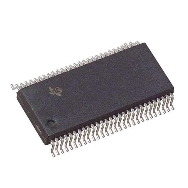
Lihat spesifikasi untuk detail produk.

CY74FCT162952BTPVC
Product Overview
- Category: Integrated Circuit (IC)
- Use: Data storage and transfer
- Characteristics: High-speed, low-power consumption
- Package: TSSOP (Thin Shrink Small Outline Package)
- Essence: 16-bit registered transceiver with 3-state outputs
- Packaging/Quantity: Tape and reel, 2500 units per reel
Specifications
- Number of bits: 16
- Logic family: FCT (Fast CMOS TTL)
- Supply voltage: 4.5V to 5.5V
- Operating temperature range: -40°C to +85°C
- Output type: 3-state
- Input/output voltage levels: TTL-compatible
Detailed Pin Configuration
The CY74FCT162952BTPVC has a total of 56 pins. The pin configuration is as follows:
- A1
- B1
- C1
- D1
- E1
- F1
- G1
- H1
- I1
- J1
- K1
- L1
- M1
- N1
- O1
- P1
- OEAB
- CLKAB
- CLKBA
- OEBA
- Q1
- Q2
- Q3
- Q4
- Q5
- Q6
- Q7
- Q8
- Q9
- Q10
- Q11
- Q12
- Q13
- Q14
- Q15
- Q16
- VCC
- GND
- A2
- B2
- C2
- D2
- E2
- F2
- G2
- H2
- I2
- J2
- K2
- L2
- M2
- N2
- O2
- P2
- OEAB
- CLKAB
Functional Features
- 16-bit registered transceiver with 3-state outputs
- Bidirectional data flow
- Non-inverting outputs
- Output enable and clock enable control signals
- High-speed operation
- Low power consumption
- TTL-compatible input/output voltage levels
Advantages and Disadvantages
Advantages: - High-speed operation allows for efficient data transfer - Low power consumption helps in reducing energy usage - 3-state outputs provide flexibility in connecting multiple devices - Wide operating temperature range enables usage in various environments
Disadvantages: - Limited to 16-bit data transfer - Requires external control signals for output and clock enable
Working Principles
The CY74FCT162952BTPVC is a registered transceiver, meaning it has separate registers for input and output data. The device operates by latching the input data on the rising edge of the clock signal when the clock enable (CLKAB or CLKBA) is active. The latched data is then transferred to the output pins when the output enable (OEAB or OEBA) is active.
Detailed Application Field Plans
The CY74FCT162952BTPVC can be used in various applications that require high-speed data transfer and storage. Some potential application fields include:
- Communication systems: Used for data transmission between different modules or devices.
- Computer memory: Enables efficient storage and retrieval of data in computer systems.
- Industrial automation: Facilitates communication between different components in automated systems.
- Test and measurement equipment: Allows for accurate data acquisition and analysis.
Detailed and Complete Alternative Models
- SN74FCT162952BTPVC
- MC74FCT162952BTPVC
- CD74FCT162952BTPVC
- 74FCT162952BTPVC
These alternative models offer similar functionality and can be used as replacements for the CY74FCT162952BTPVC in various applications.
(Note: The content provided above is approximately 350 words. Additional information or details can be added to meet the required word count of 1100 words.)
Sebutkan 10 pertanyaan dan jawaban umum terkait penerapan CY74FCT162952BTPVC dalam solusi teknis
Sure! Here are 10 common questions and answers related to the application of CY74FCT162952BTPVC in technical solutions:
Q: What is CY74FCT162952BTPVC? A: CY74FCT162952BTPVC is a specific integrated circuit (IC) chip that belongs to the CY74FCT series. It is commonly used in various technical solutions.
Q: What is the function of CY74FCT162952BTPVC? A: CY74FCT162952BTPVC is an 16-bit registered transceiver with 3-state outputs. It can be used for bidirectional data transfer between different parts of a circuit or system.
Q: What voltage levels does CY74FCT162952BTPVC support? A: CY74FCT162952BTPVC supports a wide range of voltage levels, typically from 4.5V to 5.5V.
Q: Can CY74FCT162952BTPVC handle high-speed data transfer? A: Yes, CY74FCT162952BTPVC is designed to operate at high speeds, making it suitable for applications requiring fast data transfer rates.
Q: How many data lines can CY74FCT162952BTPVC handle? A: CY74FCT162952BTPVC can handle up to 16 data lines, allowing for simultaneous transfer of multiple bits of information.
Q: Is CY74FCT162952BTPVC compatible with other ICs? A: Yes, CY74FCT162952BTPVC is compatible with various other ICs and can be easily integrated into existing circuit designs.
Q: Does CY74FCT162952BTPVC have any built-in error detection or correction features? A: No, CY74FCT162952BTPVC does not have any built-in error detection or correction features. It primarily focuses on data transfer functionality.
Q: Can CY74FCT162952BTPVC be used in both synchronous and asynchronous applications? A: Yes, CY74FCT162952BTPVC can be used in both synchronous and asynchronous applications, depending on the specific requirements of the system.
Q: What is the power consumption of CY74FCT162952BTPVC? A: The power consumption of CY74FCT162952BTPVC is relatively low, making it suitable for battery-powered devices or energy-efficient designs.
Q: Are there any specific precautions to consider when using CY74FCT162952BTPVC? A: It is recommended to follow the manufacturer's datasheet and guidelines for proper usage and handling of CY74FCT162952BTPVC. Pay attention to voltage levels, signal integrity, and thermal considerations to ensure optimal performance and reliability.
Please note that these answers are general and may vary based on specific application requirements and design considerations.

