

Lihat spesifikasi untuk detail produk.
CDCLVC1102PW
Overview
CDCLVC1102PW is a product belonging to the category of integrated circuits. It is commonly used in electronic devices for signal conditioning and clock distribution purposes. The CDCLVC1102PW offers various characteristics that make it suitable for these applications. It comes in a small package, making it easy to integrate into different circuit designs. The essence of this product lies in its ability to provide precise clock signals with low jitter and skew.
Specifications and Parameters
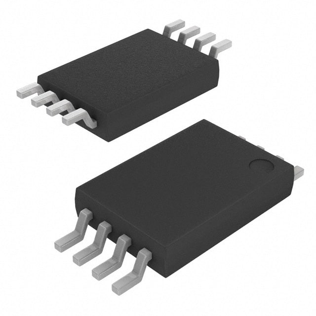
- Package: PW (TSSOP)
- Quantity per package: 1 piece
- Supply voltage range: 2.3V to 3.6V
- Operating temperature range: -40°C to +85°C
- Output frequency range: Up to 200 MHz
- Input frequency range: Up to 400 MHz
Pin Configuration
The CDCLVC1102PW has a detailed and complete pin configuration as follows:
- VDD
- GND
- OUT0
- OUT1
- OUT2
- OUT3
- IN0
- IN1
- SEL
- OE
Functional Characteristics
The CDCLVC1102PW provides the following functional characteristics:
- Low output skew and jitter
- High-speed clock distribution
- Selectable input frequency
- Output enable/disable control
- Wide supply voltage range
- ESD protection on all pins
Advantages and Disadvantages
Advantages: - Precise clock signal generation - Low skew and jitter - Small package size - Wide operating temperature range
Disadvantages: - Limited output frequency range - Requires external components for certain applications
Applicable Range of Products
The CDCLVC1102PW is commonly used in various electronic devices that require clock distribution and signal conditioning. It finds applications in telecommunications, networking equipment, data centers, and consumer electronics.
Working Principles
The CDCLVC1102PW operates by taking an input clock signal and distributing it to multiple output channels with low skew and jitter. It incorporates internal circuitry to condition the input signal and provide precise clock outputs. The selectable input frequency and output enable/disable control enhance its flexibility in different applications.
Detailed Application Field Plans
The CDCLVC1102PW can be used in the following application fields:
- Networking switches: for clock distribution among different components.
- Data storage systems: for synchronizing data transfer operations.
- Test and measurement equipment: for generating accurate timing signals.
- Audio/video equipment: for synchronization of audio and video streams.
- Industrial automation: for precise timing in control systems.
Detailed Alternative Models
Some alternative models to the CDCLVC1102PW include:
- CDCLVC1101PW
- CDCLVC1103PW
- CDCLVC1104PW
- CDCLVC1105PW
- CDCLVC1106PW
5 Common Technical Questions and Answers
Q: What is the maximum output frequency of the CDCLVC1102PW? A: The CDCLVC1102PW can support output frequencies up to 200 MHz.
Q: Can I use this product with a supply voltage below 2.3V? A: No, the CDCLVC1102PW requires a supply voltage between 2.3V and 3.6V.
Q: How many output channels does the CDCLVC1102PW have? A: The CDCLVC1102PW has four output channels labeled OUT0, OUT1, OUT2, and OUT3.
Q: Is there any protection against electrostatic discharge (ESD)? A: Yes, the CDCLVC1102PW features ESD protection on all of its pins.
Q: Can I disable the output of the CDCLVC1102PW? A: Yes, the CDCLVC1102PW has an output enable/disable control pin (OE) for this purpose.
This concludes the encyclopedia entry for CDCLVC1102PW.