

Lihat spesifikasi untuk detail produk.
CDCI6214RGET
Overview
Category: Integrated Circuit (IC)
Use: Clock Generator
Characteristics: - Generates clock signals for digital systems - Provides precise timing for synchronous operations - Supports various clock frequencies and output formats
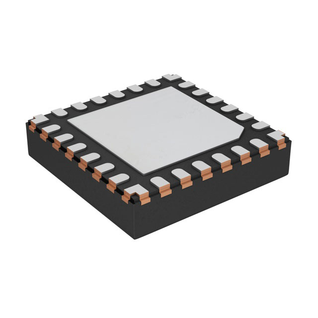
Package: QFN-16
Essence: The CDCI6214RGET is a clock generator IC designed to provide accurate and reliable clock signals for digital systems.
Packaging/Quantity: The CDCI6214RGET is available in a QFN-16 package. Each package contains one IC.
Specifications and Parameters
- Input Voltage Range: 2.5V - 3.3V
- Output Frequency Range: 1MHz - 200MHz
- Output Format: LVCMOS
- Operating Temperature Range: -40°C to +85°C
Pin Configuration
The CDCI6214RGET features the following pin configuration:
| Pin Number | Pin Name | Description | |------------|----------|-------------| | 1 | VDD | Power Supply Voltage | | 2 | GND | Ground | | 3 | OUT0 | Clock Output 0 | | 4 | OUT1 | Clock Output 1 | | 5 | OUT2 | Clock Output 2 | | 6 | OUT3 | Clock Output 3 | | 7 | OE | Output Enable | | 8 | SEL0 | Frequency Selection Bit 0 | | 9 | SEL1 | Frequency Selection Bit 1 | | 10 | SEL2 | Frequency Selection Bit 2 | | 11 | SEL3 | Frequency Selection Bit 3 | | 12 | SEL4 | Frequency Selection Bit 4 | | 13 | SEL5 | Frequency Selection Bit 5 | | 14 | SEL6 | Frequency Selection Bit 6 | | 15 | SEL7 | Frequency Selection Bit 7 | | 16 | VDD | Power Supply Voltage |
Functional Characteristics
- Generates clock signals with precise frequency and phase
- Supports multiple output frequencies simultaneously
- Output enable/disable control for power-saving operation
- Easy frequency selection through dedicated pins
- Low jitter and high accuracy
Advantages and Disadvantages
Advantages: - Accurate and reliable clock generation - Flexible frequency selection - Low power consumption - Compact package size
Disadvantages: - Limited output frequency range - Requires external frequency selection configuration
Applicable Range of Products
The CDCI6214RGET is suitable for a wide range of digital systems that require precise clock signals, such as: - Microcontrollers - Digital signal processors - FPGAs - Communication devices - Consumer electronics
Working Principles
The CDCI6214RGET utilizes an internal oscillator and frequency dividers to generate clock signals. The frequency selection bits determine the output frequency by controlling the division ratio. The output enable pin allows for easy power management by enabling or disabling the clock outputs.
Detailed Application Field Plans
The CDCI6214RGET can be used in various applications, including: 1. Microcontroller-based systems requiring accurate timing synchronization. 2. FPGA-based designs where multiple clock frequencies are needed. 3. Communication devices that rely on precise clock signals for data transmission. 4. Consumer electronics, such as digital cameras and audio/video equipment, that require synchronized operations. 5. Industrial automation systems that demand reliable clock sources for process control.
Detailed Alternative Models
Some alternative models to the CDCI6214RGET include: - CDCI6214RGZT - CDCI6214RHAT - CDCI6214RHBT
5 Common Technical Questions and Answers
Q: What is the maximum output frequency of the CDCI6214RGET? A: The CDCI6214RGET can generate clock signals with a maximum frequency of 200MHz.
Q: Can I use the CDCI6214RGET in a 3.3V system? A: Yes, the CDCI6214RGET supports an input voltage range of 2.5V to 3.3V.
Q: How many clock outputs does the CDCI6214RGET have? A: The CDCI6214RGET has four clock outputs: OUT0, OUT1, OUT2, and OUT3.
Q: Is the CDCI6214RGET suitable for battery-powered devices? A: Yes, the CDCI6214RGET features low power consumption, making it suitable for battery-powered applications.
Q: Can I disable the clock outputs when not in use? A: Yes