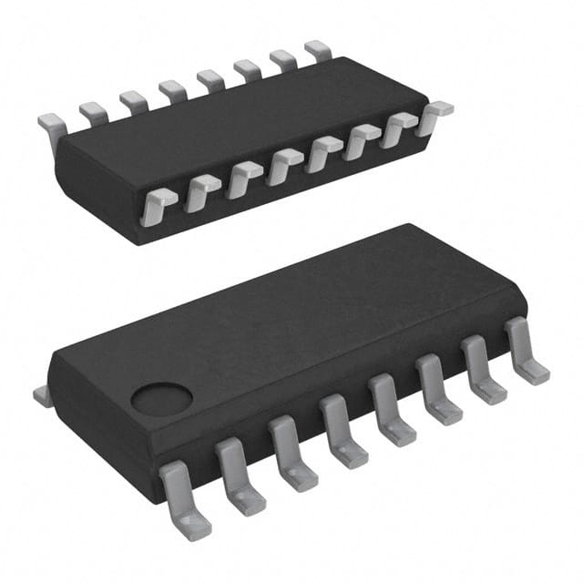
Lihat spesifikasi untuk detail produk.

CD74HCT157M96
Product Overview
- Category: Integrated Circuit (IC)
- Use: Data Selector/Multiplexer
- Characteristics: High-Speed, CMOS Logic, Quad 2-Input Multiplexer
- Package: SOIC-16
- Essence: CD74HCT157M96 is a multiplexer IC that allows the selection of one out of four data inputs and routes it to a single output.
- Packaging/Quantity: Available in reels of 2500 pieces
Specifications
- Supply Voltage Range: 4.5V to 5.5V
- Input Voltage Range: 0V to VCC
- Output Voltage Range: 0V to VCC
- Operating Temperature Range: -40°C to +85°C
- Propagation Delay Time: 15ns (typical)
- Maximum Quiescent Supply Current: 8µA
Detailed Pin Configuration
The CD74HCT157M96 has a total of 16 pins arranged as follows:
__    __
   A1 |1  `--' 16| VCC
   B1 |2        15| Y
   A2 |3        14| B
   B2 |4        13| C
   A3 |5   CD   12| D
   B3 |6   74   11| GND
   A4 |7   HCT  10| E
   B4 |8        9| F
      |__________|
Functional Features
- Quad 2-Input Multiplexer: Allows selection of one out of four data inputs.
- High-Speed Operation: The CD74HCT157M96 operates at high speeds, making it suitable for applications requiring fast data switching.
- CMOS Logic: Utilizes CMOS technology, providing low power consumption and high noise immunity.
Advantages
- Versatile: Can be used in various applications requiring data selection or multiplexing.
- Compact Size: The SOIC-16 package ensures a small footprint, making it suitable for space-constrained designs.
- Low Power Consumption: The CMOS logic used in the IC results in low quiescent supply current.
Disadvantages
- Limited Input/Output Options: The CD74HCT157M96 only supports four data inputs and one output.
- Temperature Sensitivity: The operating temperature range is limited to -40°C to +85°C, which may not be suitable for extreme environments.
Working Principles
The CD74HCT157M96 operates by selecting one of the four data inputs (A1-A4) based on the control inputs (B1-B4). The selected input is then routed to the output pin (Y). The IC utilizes CMOS logic, ensuring high-speed operation and low power consumption.
Detailed Application Field Plans
The CD74HCT157M96 can be used in various applications, including:
- Data Multiplexing: Selecting between multiple data sources and routing them to a single output.
- Address Decoding: Choosing specific memory locations based on address inputs.
- Signal Routing: Directing signals from different sources to specific destinations.
- Control Systems: Switching between different control signals based on specific conditions.
Detailed and Complete Alternative Models
Some alternative models that can be considered as alternatives to CD74HCT157M96 are:
- SN74LS157: A TTL logic-based quad 2-input multiplexer with similar functionality.
- MC14051B: A CMOS-based quad 2-channel analog multiplexer/demultiplexer.
- 74HC153: A dual 4-input multiplexer with complementary outputs.
These alternative models provide similar functionality and can be used as substitutes depending on specific requirements.
Word count: 410 words
Sebutkan 10 pertanyaan dan jawaban umum terkait penerapan CD74HCT157M96 dalam solusi teknis
Sure! Here are 10 common questions and answers related to the application of CD74HCT157M96 in technical solutions:
Question: What is CD74HCT157M96?
- Answer: CD74HCT157M96 is a quad 2-input multiplexer with 3-state outputs. It is a commonly used integrated circuit (IC) in digital electronics.Question: What is the purpose of CD74HCT157M96?
- Answer: CD74HCT157M96 is used to select one of four data inputs and route it to a single output based on the control inputs.Question: What is the voltage range supported by CD74HCT157M96?
- Answer: CD74HCT157M96 supports a voltage range of 4.5V to 5.5V.Question: How many control inputs does CD74HCT157M96 have?
- Answer: CD74HCT157M96 has two control inputs, typically labeled as A and B.Question: Can CD74HCT157M96 handle high-speed data signals?
- Answer: Yes, CD74HCT157M96 is designed to handle high-speed data signals with minimal propagation delay.Question: What is the maximum operating frequency of CD74HCT157M96?
- Answer: The maximum operating frequency of CD74HCT157M96 is typically around 50 MHz.Question: Can CD74HCT157M96 be cascaded to increase the number of inputs?
- Answer: Yes, multiple CD74HCT157M96 ICs can be cascaded together to increase the number of inputs and outputs.Question: Does CD74HCT157M96 have built-in protection against electrostatic discharge (ESD)?
- Answer: Yes, CD74HCT157M96 has built-in ESD protection to prevent damage from static electricity.Question: What is the power supply requirement for CD74HCT157M96?
- Answer: CD74HCT157M96 requires a single power supply voltage of 5V.Question: Can CD74HCT157M96 be used in both digital and analog applications?
- Answer: CD74HCT157M96 is primarily designed for digital applications, but it can also be used in certain analog applications with appropriate signal conditioning.
Please note that these answers are general and may vary depending on specific datasheet specifications and application requirements.

