Lihat spesifikasi untuk detail produk.

CD74HC4049PWR
Product Overview
- Category: Integrated Circuit
- Use: Signal Conversion and Level Shifting
- Characteristics: High-Speed, CMOS Logic, Hex Inverting Buffer/Converter
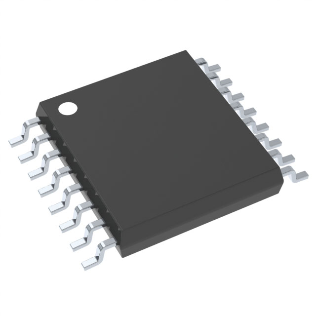
- Package: TSSOP (Thin Shrink Small Outline Package)
- Essence: Hex Inverter with Enhanced ESD Protection
- Packaging/Quantity: Tape and Reel, 2500 pieces per reel
Specifications
The CD74HC4049PWR is a high-speed CMOS logic integrated circuit that serves as a hex inverting buffer/converter. It operates on a wide voltage range from 2V to 6V, making it suitable for various applications. The device offers enhanced electrostatic discharge (ESD) protection, ensuring reliable performance even in challenging environments.
Detailed Pin Configuration
The CD74HC4049PWR package consists of a total of 16 pins. The pin configuration is as follows:
- Pin 1: Input A1
- Pin 2: Output Y1
- Pin 3: Input A2
- Pin 4: Output Y2
- Pin 5: Input A3
- Pin 6: Output Y3
- Pin 7: Ground (GND)
- Pin 8: Output Y4
- Pin 9: Input A4
- Pin 10: Output Y5
- Pin 11: Input A5
- Pin 12: Output Y6
- Pin 13: VCC (Positive Power Supply)
- Pin 14: Input A6
- Pin 15: Output Y7
- Pin 16: Input A7
Functional Features
The CD74HC4049PWR provides the following functional features:
- Hex inverting buffer/converter with high-speed operation.
- Wide voltage range (2V to 6V) for compatibility with various systems.
- Enhanced ESD protection for improved reliability.
- Low power consumption, making it suitable for battery-powered applications.
- High noise immunity, ensuring stable operation in noisy environments.
Advantages and Disadvantages
Advantages of the CD74HC4049PWR include:
- High-speed operation allows for efficient signal conversion.
- Wide voltage range enables compatibility with different voltage levels.
- Enhanced ESD protection ensures reliable performance in challenging conditions.
- Low power consumption makes it suitable for energy-efficient designs.
- High noise immunity provides stable operation in noisy environments.
Disadvantages of the CD74HC4049PWR include:
- Limited number of input/output channels (6 inverters).
- Not suitable for applications requiring a large number of logic gates.
- May not be cost-effective for low-volume production.
Working Principles
The CD74HC4049PWR operates based on CMOS (Complementary Metal-Oxide-Semiconductor) technology. It utilizes a combination of P-channel and N-channel MOSFETs to achieve high-speed logic operations. The hex inverting buffer/converter configuration allows for easy signal inversion and level shifting.
Detailed Application Field Plans
The CD74HC4049PWR finds applications in various fields, including:
- Digital Communication Systems: Signal conversion and level shifting in data transmission circuits.
- Industrial Automation: Interface between different voltage levels in control systems.
- Consumer Electronics: Signal processing and level translation in audio/video equipment.
- Automotive Electronics: Voltage level adaptation in automotive communication networks.
- Medical Devices: Signal conditioning and conversion in medical monitoring equipment.
Detailed and Complete Alternative Models
Some alternative models that can be considered as replacements for the CD74HC4049PWR are:
- SN74HC04N: Hex Inverter, DIP package.
- CD4049UBE: CMOS Hex Inverting Buffer/Converter, PDIP package.
- MC74HC4049DR2G: High-Speed CMOS Logic Hex Inverting Buffer/Converter, SOIC package.
These alternative models offer similar functionality and can be used as drop-in replacements in many applications.
Word count: 383 words
Sebutkan 10 pertanyaan dan jawaban umum terkait penerapan CD74HC4049PWR dalam solusi teknis
Sure! Here are 10 common questions and answers related to the application of CD74HC4049PWR:
Q: What is CD74HC4049PWR? A: CD74HC4049PWR is a hex inverter/buffer IC (integrated circuit) that is commonly used in digital logic applications.
Q: What is the operating voltage range for CD74HC4049PWR? A: The operating voltage range for CD74HC4049PWR is typically between 2V and 6V.
Q: What is the maximum output current of CD74HC4049PWR? A: The maximum output current of CD74HC4049PWR is around 5mA.
Q: Can CD74HC4049PWR be used as a level shifter? A: Yes, CD74HC4049PWR can be used as a level shifter to convert signals between different voltage levels.
Q: How many inverters are there in CD74HC4049PWR? A: CD74HC4049PWR contains six independent inverters.
Q: What is the typical propagation delay of CD74HC4049PWR? A: The typical propagation delay of CD74HC4049PWR is around 11 ns.
Q: Can CD74HC4049PWR drive capacitive loads? A: Yes, CD74HC4049PWR can drive small capacitive loads without any additional buffering.
Q: Is CD74HC4049PWR compatible with TTL (Transistor-Transistor Logic) inputs? A: Yes, CD74HC4049PWR is compatible with TTL inputs and can be used as a drop-in replacement for TTL inverters.
Q: Can CD74HC4049PWR be used in high-speed applications? A: Yes, CD74HC4049PWR is suitable for high-speed applications due to its low propagation delay and high-speed operation.
Q: What is the package type of CD74HC4049PWR? A: CD74HC4049PWR is available in a small outline TSSOP (Thin Shrink Small Outline Package) package.
Please note that the answers provided here are general and may vary depending on specific datasheet specifications and application requirements.

