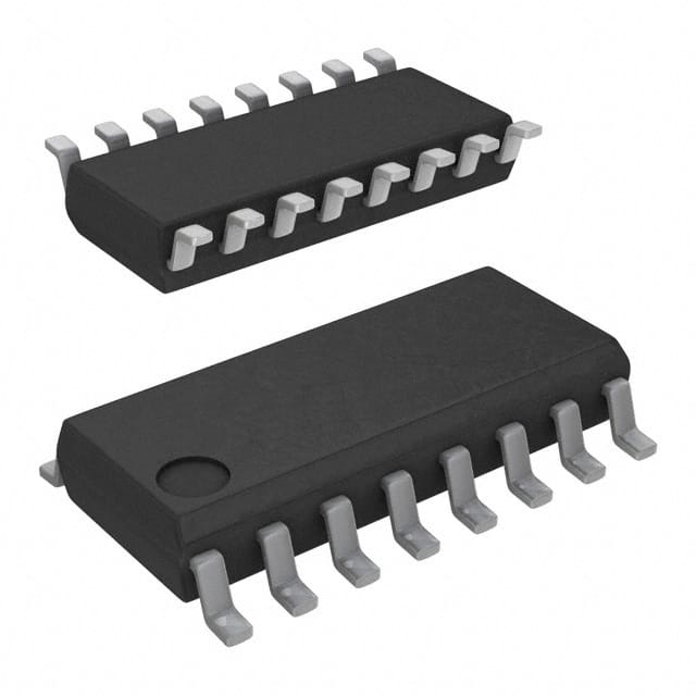
Lihat spesifikasi untuk detail produk.

CD74HC151M96
Product Overview
- Category: Integrated Circuit (IC)
- Use: Data Selector/Multiplexer
- Characteristics: High-Speed, CMOS Logic, 8:1 Multiplexer
- Package: SOIC-16
- Essence: The CD74HC151M96 is a high-speed CMOS logic IC that functions as an 8:1 multiplexer. It is commonly used in digital systems to select one of eight input data lines and route it to the output line based on the control inputs.
- Packaging/Quantity: The CD74HC151M96 is available in a standard SOIC-16 package and is typically sold in reels or tubes containing multiple units.
Specifications
- Supply Voltage Range: 2V to 6V
- Input Voltage Range: 0V to VCC
- Output Voltage Range: 0V to VCC
- Operating Temperature Range: -40°C to +85°C
- Propagation Delay: 13 ns (typical)
- Input Capacitance: 3.5 pF (typical)
- Output Current: ±25 mA
Pin Configuration
The CD74HC151M96 has a total of 16 pins arranged in a dual in-line package (DIP). The pin configuration is as follows:
+---+--+---+
   A0  |1  +--+ 16| VCC
   A1  |2       15| B
   A2  |3       14| C
   A3  |4       13| D
   A4  |5  CD74HC151M96 12| E
   A5  |6       11| F
   A6  |7       10| G
   A7  |8        9| H
       +----------+
Functional Features
- 8:1 Data Selector/Multiplexer
- High-Speed CMOS Logic
- Low Power Consumption
- Wide Operating Voltage Range
- Schmitt Trigger Inputs for Noise Immunity
- Output Current Protection
- TTL-Compatible Inputs and Outputs
Advantages and Disadvantages
Advantages: - High-speed operation allows for efficient data selection in digital systems. - CMOS logic provides low power consumption and wide operating voltage range. - Schmitt trigger inputs enhance noise immunity, ensuring reliable operation. - Output current protection prevents damage to the IC and connected devices. - Compatibility with TTL logic levels simplifies integration into existing systems.
Disadvantages: - Limited to 8:1 multiplexing capability, may not be suitable for applications requiring higher input/output configurations. - Propagation delay of 13 ns may introduce timing constraints in certain high-speed applications.
Working Principles
The CD74HC151M96 operates based on the principle of data selection using control inputs. The eight input lines (A0-A7) carry data signals, while the control inputs (B, C, D, E) determine which input line is selected and routed to the output line (F). The selected input is determined by the binary value applied to the control inputs.
Detailed Application Field Plans
The CD74HC151M96 finds application in various digital systems where data selection or multiplexing is required. Some common application fields include:
- Digital Communication Systems: Used for selecting different data sources in communication protocols such as UART, SPI, or I2C.
- Data Acquisition Systems: Enables the selection of multiple analog or digital sensors for data acquisition purposes.
- Multiplexed Displays: Allows for the selection of different display segments in multiplexed display systems, such as 7-segment displays.
- Memory Addressing: Used in memory systems to select different memory banks or address lines.
Detailed and Complete Alternative Models
- SN74HC151: Similar 8:1 multiplexer IC from Texas Instruments with comparable specifications.
- CD4051B: Analog multiplexer/demultiplexer IC that can also be used for data selection purposes.
- MC14051B: CMOS analog multiplexer/demultiplexer IC with multiple channels for data routing applications.
These alternative models offer similar functionality and can be considered as alternatives to the CD74HC151M96 based on specific requirements and availability.
Word count: 511 words
Sebutkan 10 pertanyaan dan jawaban umum terkait penerapan CD74HC151M96 dalam solusi teknis
Sure! Here are 10 common questions and answers related to the application of CD74HC151M96 in technical solutions:
Q: What is CD74HC151M96? A: CD74HC151M96 is a 8-input multiplexer (MUX) integrated circuit (IC) that can be used to select one of eight data inputs based on a control signal.
Q: What is the operating voltage range for CD74HC151M96? A: CD74HC151M96 operates within a voltage range of 2V to 6V.
Q: What is the maximum frequency at which CD74HC151M96 can operate? A: CD74HC151M96 has a maximum operating frequency of 50 MHz.
Q: How many data inputs does CD74HC151M96 have? A: CD74HC151M96 has 8 data inputs labeled D0 to D7.
Q: How is the input selection controlled in CD74HC151M96? A: The input selection is controlled by a 3-bit binary control signal, which determines the active input.
Q: Can CD74HC151M96 be cascaded to increase the number of inputs? A: Yes, CD74HC151M96 can be cascaded to increase the number of inputs by connecting the outputs of one MUX to the inputs of another.
Q: What is the output format of CD74HC151M96? A: CD74HC151M96 provides a single output line that carries the selected input data.
Q: What is the power supply requirement for CD74HC151M96? A: CD74HC151M96 requires a power supply voltage between 2V and 6V.
Q: What is the typical power consumption of CD74HC151M96? A: The typical power consumption of CD74HC151M96 is around 10mW.
Q: What are some common applications of CD74HC151M96? A: CD74HC151M96 can be used in various applications such as data multiplexing, signal routing, address decoding, and data selection in digital systems.
Please note that these answers are general and may vary depending on the specific requirements and datasheet of CD74HC151M96.

