

Lihat spesifikasi untuk detail produk.
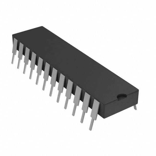
CD4097BE
Product Overview
- Category: Integrated Circuit
- Use: Digital Multiplexer/Demultiplexer
- Characteristics: High-speed, low-power consumption
- Package: DIP (Dual In-line Package)
- Essence: CMOS (Complementary Metal-Oxide-Semiconductor) technology
- Packaging/Quantity: Tube packaging, 25 pieces per tube
Specifications
The CD4097BE is a digital multiplexer/demultiplexer integrated circuit. It operates using CMOS technology, which provides high-speed performance while consuming low power. The device comes in a Dual In-line Package (DIP) and is packaged in tubes containing 25 pieces each.
Detailed Pin Configuration
The CD4097BE has a total of 16 pins, each serving a specific function. The pin configuration is as follows:
- Pin 1: VDD - Positive Power Supply
- Pin 2: A0 - Address Input
- Pin 3: A1 - Address Input
- Pin 4: A2 - Address Input
- Pin 5: A3 - Address Input
- Pin 6: E - Enable Input
- Pin 7: Y0 - Output
- Pin 8: Y1 - Output
- Pin 9: Y2 - Output
- Pin 10: Y3 - Output
- Pin 11: Y4 - Output
- Pin 12: Y5 - Output
- Pin 13: Y6 - Output
- Pin 14: Y7 - Output
- Pin 15: GND - Ground
- Pin 16: NC - No Connection
Functional Features
The CD4097BE functions as a digital multiplexer/demultiplexer. It allows for the selection of one of eight input lines to be routed to a single output line. The device can also operate in the demultiplexing mode, where a single input line is routed to one of eight output lines based on the address inputs.
Advantages and Disadvantages
Advantages: - High-speed performance - Low power consumption - Versatile functionality as both a multiplexer and demultiplexer - Compact DIP package for easy integration
Disadvantages: - Limited number of input/output lines (8) - Requires external control signals for operation
Working Principles
The CD4097BE operates based on CMOS technology, which utilizes complementary pairs of MOSFETs (Metal-Oxide-Semiconductor Field-Effect Transistors) to achieve high-speed switching and low power consumption. The device uses address inputs to select the desired input/output line combination and an enable input to control the operation.
Detailed Application Field Plans
The CD4097BE finds applications in various fields where digital multiplexing/demultiplexing is required. Some potential application areas include:
- Data communication systems
- Telecommunication equipment
- Industrial automation
- Instrumentation and measurement devices
- Audio/video signal routing systems
Detailed and Complete Alternative Models
There are several alternative models available that offer similar functionality to the CD4097BE. Some popular alternatives include:
- CD4051B - 8-Channel Analog Multiplexer/Demultiplexer
- CD4067B - 16-Channel Analog Multiplexer/Demultiplexer
- CD74HC4067 - 16-Channel Analog Multiplexer/Demultiplexer
- CD4052B - Dual 4-Channel Analog Multiplexer/Demultiplexer
These alternative models provide different channel configurations and may have varying specifications, but they serve the same purpose of digital multiplexing/demultiplexing.
In conclusion, the CD4097BE is a versatile integrated circuit that operates as a digital multiplexer/demultiplexer. It offers high-speed performance, low power consumption, and comes in a compact DIP package. The device finds applications in various fields such as data communication, telecommunication, industrial automation, and more. Alternative models with different channel configurations are also available for specific requirements.
Sebutkan 10 pertanyaan dan jawaban umum terkait penerapan CD4097BE dalam solusi teknis
Sure! Here are 10 common questions and answers related to the application of CD4097BE in technical solutions:
Q: What is CD4097BE? A: CD4097BE is a CMOS analog multiplexer/demultiplexer integrated circuit (IC) that can be used for various switching applications.
Q: What is the operating voltage range of CD4097BE? A: The operating voltage range of CD4097BE is typically between 3V and 18V.
Q: How many channels does CD4097BE have? A: CD4097BE has 8 channels, which means it can switch between 8 different inputs or outputs.
Q: Can CD4097BE handle both analog and digital signals? A: Yes, CD4097BE can handle both analog and digital signals, making it versatile for various applications.
Q: What is the maximum frequency range supported by CD4097BE? A: CD4097BE can support frequencies up to several megahertz, depending on the specific application and conditions.
Q: Can CD4097BE be cascaded to increase the number of channels? A: Yes, multiple CD4097BE ICs can be cascaded together to increase the number of channels as required.
Q: Does CD4097BE have built-in protection features? A: CD4097BE does not have built-in protection features, so external measures may be needed to protect against overvoltage or ESD.
Q: What is the typical power consumption of CD4097BE? A: The typical power consumption of CD4097BE is relatively low, making it suitable for battery-powered applications.
Q: Can CD4097BE be used in both analog and digital multiplexing applications? A: Yes, CD4097BE can be used for both analog and digital multiplexing applications, providing flexibility in design.
Q: Are there any specific considerations for using CD4097BE in high-speed applications? A: In high-speed applications, it is important to consider the propagation delay and signal integrity to ensure proper operation of CD4097BE.
Please note that these answers are general and may vary depending on the specific application and requirements.