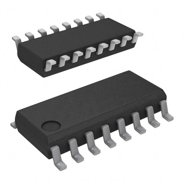
Lihat spesifikasi untuk detail produk.

CD40257BM96G4
Product Overview
- Category: Integrated Circuit (IC)
- Use: Multiplexer/Demultiplexer
- Characteristics: High-speed, low-power consumption
- Package: SOIC-16
- Essence: Digital logic IC for data routing and selection
- Packaging/Quantity: Tape and Reel, 2500 units per reel
Specifications
- Supply Voltage: 3V to 18V
- Logic Family: CMOS
- Number of Channels: 1
- Input Compatibility: TTL, CMOS
- Operating Temperature Range: -40°C to +85°C
- Propagation Delay: 15ns (typical)
- Output Current: ±8mA
- Power Dissipation: 10mW (typical)
Detailed Pin Configuration
The CD40257BM96G4 has a total of 16 pins. The pin configuration is as follows:
- A0: Address Input
- A1: Address Input
- A2: Address Input
- A3: Address Input
- I: Data Input
- B: Data Input
- C: Data Input
- D: Data Input
- E: Data Input
- F: Data Input
- G: Data Input
- H: Data Input
- Y: Multiplexed Output
- VCC: Positive Supply Voltage
- GND: Ground
- OE: Output Enable
Functional Features
- 1-to-8 multiplexer/demultiplexer functionality
- Low power consumption
- Wide operating voltage range
- Fast switching speed
- High noise immunity
- Break-before-make switching action
Advantages and Disadvantages
Advantages
- Versatile multiplexer/demultiplexer functionality
- Low power consumption makes it suitable for battery-powered devices
- Wide operating voltage range allows compatibility with various systems
- Fast switching speed enables high-speed data routing
- High noise immunity ensures reliable operation in noisy environments
Disadvantages
- Limited number of channels (1)
- Propagation delay may affect real-time applications
Working Principles
The CD40257BM96G4 is a digital logic IC that functions as a 1-to-8 multiplexer/demultiplexer. It routes or selects data from one of the eight input lines to the output line based on the address inputs. The output can be enabled or disabled using the OE pin. The IC operates on CMOS technology, providing low power consumption and high noise immunity.
Detailed Application Field Plans
The CD40257BM96G4 finds applications in various fields, including:
- Data communication systems
- Telecommunications equipment
- Industrial automation
- Test and measurement instruments
- Consumer electronics
- Automotive electronics
- Medical devices
- Security systems
Detailed and Complete Alternative Models
Some alternative models to the CD40257BM96G4 include:
- SN74HC257N: 1-to-8 Line Data Selector/Multiplexer/Demultiplexer
- CD74HC257E: High-Speed CMOS Logic 1-to-8 Line Data Selector/Multiplexer/Demultiplexer
- MC74HC257N: Quad 2-Input Multiplexer
These alternatives offer similar functionality and can be used as replacements depending on specific requirements.
Word count: 346 words
Sebutkan 10 pertanyaan dan jawaban umum terkait penerapan CD40257BM96G4 dalam solusi teknis
Sure! Here are 10 common questions and answers related to the application of CD40257BM96G4 in technical solutions:
Q: What is CD40257BM96G4? A: CD40257BM96G4 is a quad 2-input multiplexer with complementary outputs, commonly used in digital logic circuits.
Q: What are the key features of CD40257BM96G4? A: Some key features include low power consumption, wide supply voltage range, high noise immunity, and compatibility with various logic families.
Q: How can CD40257BM96G4 be used in technical solutions? A: CD40257BM96G4 can be used for data routing, signal selection, and multiplexing applications in digital systems.
Q: What is the operating voltage range for CD40257BM96G4? A: The operating voltage range for CD40257BM96G4 is typically between 3V and 18V.
Q: Can CD40257BM96G4 handle analog signals? A: No, CD40257BM96G4 is designed for digital signals only and cannot handle analog signals.
Q: What is the maximum frequency at which CD40257BM96G4 can operate? A: CD40257BM96G4 can typically operate at frequencies up to several megahertz (MHz).
Q: Does CD40257BM96G4 have built-in protection against electrostatic discharge (ESD)? A: Yes, CD40257BM96G4 has built-in ESD protection to prevent damage during handling and assembly.
Q: Are there any specific precautions to consider when using CD40257BM96G4? A: It is important to follow the recommended operating conditions, such as voltage levels and temperature ranges, specified in the datasheet.
Q: Can CD40257BM96G4 be cascaded to increase the number of inputs? A: Yes, multiple CD40257BM96G4 chips can be cascaded together to increase the number of inputs in a multiplexing application.
Q: Where can I find more information about CD40257BM96G4? A: You can refer to the CD40257BM96G4 datasheet provided by the manufacturer for detailed technical specifications and application notes.
Please note that the answers provided here are general and may vary depending on the specific requirements and use cases. It is always recommended to consult the datasheet and relevant technical documentation for accurate information.

