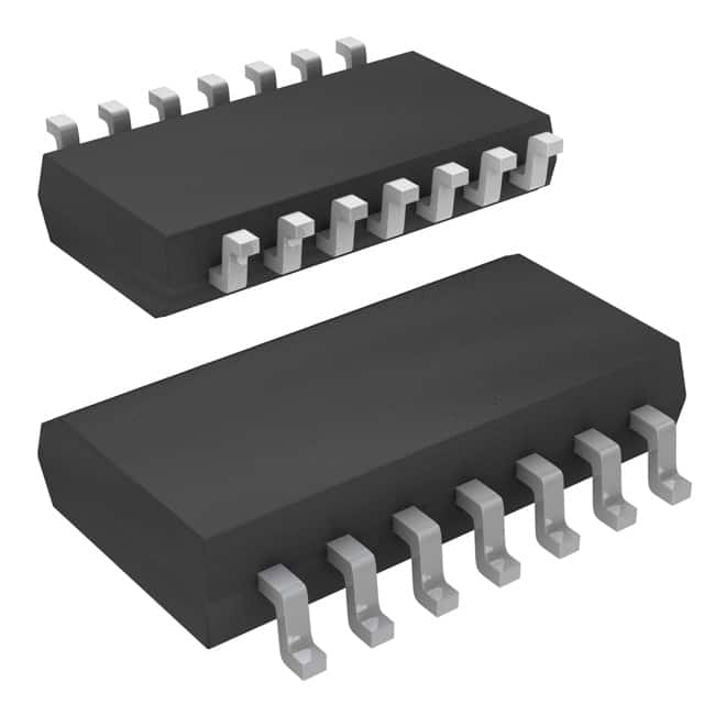
Lihat spesifikasi untuk detail produk.

CD40106BNSR
Product Overview
- Category: Integrated Circuit
- Use: Inverter Schmitt Trigger
- Characteristics: High-speed CMOS technology, low power consumption
- Package: SOIC (Small Outline Integrated Circuit)
- Essence: Hex Schmitt Trigger
- Packaging/Quantity: Tape and Reel, 2500 units per reel
Specifications
- Supply Voltage Range: 3V to 18V
- Input Voltage Range: 0V to VDD
- Output Voltage Range: 0V to VDD
- Operating Temperature Range: -55°C to +125°C
- Propagation Delay Time: 60ns (typical)
Detailed Pin Configuration
The CD40106BNSR has a total of 14 pins. The pin configuration is as follows:
- Pin 1: Input A
- Pin 2: Output A
- Pin 3: Input B
- Pin 4: Output B
- Pin 5: Input C
- Pin 6: Output C
- Pin 7: Ground (GND)
- Pin 8: Power Supply (VDD)
- Pin 9: Input D
- Pin 10: Output D
- Pin 11: Input E
- Pin 12: Output E
- Pin 13: Input F
- Pin 14: Output F
Functional Features
- Hex Schmitt Trigger with independent inverters
- Wide supply voltage range allows for versatile applications
- High noise immunity due to Schmitt trigger action
- Low power consumption makes it suitable for battery-powered devices
- Fast switching speed enables high-frequency operation
Advantages and Disadvantages
Advantages
- Versatile and widely used in various digital applications
- High noise immunity ensures reliable operation in noisy environments
- Low power consumption extends battery life in portable devices
- Fast switching speed allows for high-frequency signal processing
Disadvantages
- Limited output current capability
- Not suitable for driving heavy loads directly
- May require additional buffering or amplification for certain applications
Working Principles
The CD40106BNSR is a Hex Schmitt Trigger, which means it can convert slowly changing input signals into sharply defined digital outputs. It utilizes a positive feedback mechanism to provide hysteresis, ensuring stable and noise-immune operation. The device operates by comparing the input voltage with two threshold levels, known as the upper and lower thresholds. When the input voltage crosses these thresholds, the output switches states.
Detailed Application Field Plans
The CD40106BNSR finds applications in various fields, including:
- Oscillators and timers
- Signal conditioning and level shifting
- Pulse shaping and waveform generation
- Logic-level conversion
- Noise filtering and debouncing
- Touch-sensitive interfaces
- Voltage level detection and monitoring
Detailed and Complete Alternative Models
Some alternative models that offer similar functionality to the CD40106BNSR include:
- MC14069UBCPG: Hex Inverter Schmitt Trigger
- SN74HC14N: Hex Schmitt-Trigger Inverters
- HEF40106BT: Hex Inverting Schmitt Trigger
These alternatives can be considered based on specific requirements and availability.
Word count: 314 words
Sebutkan 10 pertanyaan dan jawaban umum terkait penerapan CD40106BNSR dalam solusi teknis
Sure! Here are 10 common questions and answers related to the application of CD40106BNSR:
Q: What is CD40106BNSR? A: CD40106BNSR is a hex inverter Schmitt trigger integrated circuit (IC) that can be used for various technical solutions.
Q: What is the operating voltage range of CD40106BNSR? A: The operating voltage range of CD40106BNSR is typically between 3V and 18V.
Q: How many inverters are there in CD40106BNSR? A: CD40106BNSR consists of six independent Schmitt trigger inverters.
Q: What is the purpose of a Schmitt trigger inverter? A: A Schmitt trigger inverter converts an input signal into a digital output signal with hysteresis, making it less sensitive to noise and providing better noise immunity.
Q: Can CD40106BNSR be used for level shifting applications? A: Yes, CD40106BNSR can be used for level shifting applications as it can convert signals from one voltage level to another.
Q: What is the maximum frequency at which CD40106BNSR can operate? A: CD40106BNSR can typically operate at frequencies up to several megahertz (MHz).
Q: Is CD40106BNSR suitable for low-power applications? A: Yes, CD40106BNSR is designed to operate at low power and has a low quiescent current consumption.
Q: Can CD40106BNSR be used for oscillator circuits? A: Yes, CD40106BNSR can be used to build simple oscillator circuits, such as relaxation oscillators or square wave generators.
Q: What is the recommended operating temperature range for CD40106BNSR? A: The recommended operating temperature range for CD40106BNSR is typically between -55°C and 125°C.
Q: Are there any specific precautions to consider when using CD40106BNSR? A: It is important to handle CD40106BNSR according to proper electrostatic discharge (ESD) precautions to avoid damage. Additionally, it is recommended to refer to the datasheet for detailed application guidelines and circuit examples.
Please note that these answers are general and may vary depending on the specific application and requirements.

