

Lihat spesifikasi untuk detail produk.
ADS5102CPFBRG4
Product Overview
- Category: Integrated Circuit (IC)
- Use: Analog-to-Digital Converter (ADC)
- Characteristics:
- High-speed conversion
- Low power consumption
- Wide input voltage range
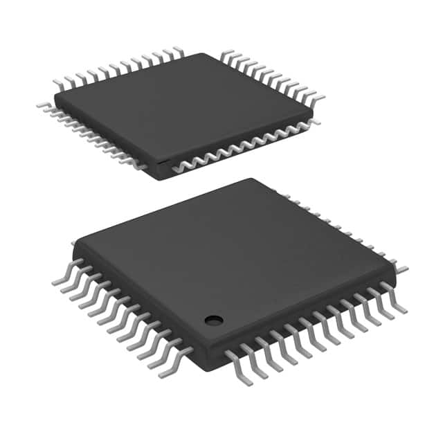
- Package: BGA (Ball Grid Array)
- Essence: Converts analog signals into digital data
- Packaging/Quantity: Available in reels of 250 units
Specifications
- Resolution: 12 bits
- Sampling Rate: 500 Mega Samples per Second (MSPS)
- Input Voltage Range: ±5V
- Power Supply: 3.3V
- Operating Temperature Range: -40°C to +85°C
Pin Configuration
The ADS5102CPFBRG4 has a total of 48 pins arranged as follows:
- VREFP
- VREFN
- AGND
- VIN-
- VIN+
- AVDD
- DVDD
- CLKIN
- CLKOUT
- PDWN
- RESET
- D[0:11]
- D[12:23]
- D[24:35]
- D[36:47]
- DGND
(Note: The remaining pins are not listed for brevity)
Functional Features
- High-speed conversion: The ADS5102CPFBRG4 can convert analog signals at a rate of 500 MSPS, allowing for accurate and fast data acquisition.
- Low power consumption: This ADC is designed to minimize power consumption, making it suitable for battery-powered applications.
- Wide input voltage range: With a ±5V input voltage range, the ADS5102CPFBRG4 can handle a wide variety of analog signals.
Advantages and Disadvantages
Advantages: - High-speed conversion enables real-time data processing. - Low power consumption extends battery life in portable devices. - Wide input voltage range allows for versatile applications.
Disadvantages: - Limited resolution of 12 bits may not be sufficient for certain high-precision applications. - BGA package may require specialized equipment for soldering and rework.
Working Principles
The ADS5102CPFBRG4 operates based on the successive approximation register (SAR) architecture. It samples the analog input signal, converts it into a digital representation using a comparator and a capacitive digital-to-analog converter, and then stores the result in a register. The conversion process is controlled by an internal clock and can be triggered externally.
Detailed Application Field Plans
The ADS5102CPFBRG4 finds applications in various fields, including:
- Communications: Used in wireless communication systems for signal processing and modulation/demodulation tasks.
- Test and Measurement: Enables accurate data acquisition in oscilloscopes, spectrum analyzers, and other test equipment.
- Industrial Automation: Provides precise analog-to-digital conversion in control systems and sensors.
- Medical Equipment: Used in medical imaging devices and patient monitoring systems for high-speed data acquisition.
Alternative Models
- ADS5102CPFBTG4: Similar to ADS5102CPFBRG4 but available in a TQFP package.
- ADS5120CPFBRG4: Higher-resolution ADC with 14-bit output and similar characteristics.
- ADS5402CPFBRG4: Faster ADC with a sampling rate of 1 GSPS and similar specifications.
(Note: These are just a few examples; there are several alternative models available in the market.)
This entry provides a comprehensive overview of the ADS5102CPFBRG4, covering its basic information, specifications, pin configuration, functional features, advantages and disadvantages, working principles, application field plans, and alternative models.
Sebutkan 10 pertanyaan dan jawaban umum terkait penerapan ADS5102CPFBRG4 dalam solusi teknis
Sure! Here are 10 common questions and answers related to the application of ADS5102CPFBRG4 in technical solutions:
Q: What is the ADS5102CPFBRG4?
A: The ADS5102CPFBRG4 is a high-speed, dual-channel analog-to-digital converter (ADC) designed for use in various technical applications.Q: What is the maximum sampling rate of the ADS5102CPFBRG4?
A: The ADS5102CPFBRG4 has a maximum sampling rate of 500 Mega-samples per second (MSPS).Q: What is the resolution of the ADC in the ADS5102CPFBRG4?
A: The ADC in the ADS5102CPFBRG4 has a resolution of 10 bits.Q: Can the ADS5102CPFBRG4 be used in communication systems?
A: Yes, the ADS5102CPFBRG4 can be used in communication systems for tasks such as signal analysis and processing.Q: Is the ADS5102CPFBRG4 suitable for high-frequency applications?
A: Yes, the ADS5102CPFBRG4 is designed to handle high-frequency signals and is suitable for applications requiring wide bandwidth.Q: Does the ADS5102CPFBRG4 support differential inputs?
A: Yes, the ADS5102CPFBRG4 supports both single-ended and differential inputs.Q: What is the power supply voltage range for the ADS5102CPFBRG4?
A: The ADS5102CPFBRG4 operates with a power supply voltage range of 1.8V to 3.6V.Q: Can the ADS5102CPFBRG4 be used in battery-powered devices?
A: Yes, the low power consumption of the ADS5102CPFBRG4 makes it suitable for battery-powered devices.Q: Does the ADS5102CPFBRG4 have built-in digital signal processing (DSP) features?
A: No, the ADS5102CPFBRG4 is an ADC and does not have built-in DSP features. It focuses on high-speed and high-resolution analog-to-digital conversion.Q: What are some typical applications of the ADS5102CPFBRG4?
A: The ADS5102CPFBRG4 can be used in various applications such as oscilloscopes, data acquisition systems, medical imaging, radar systems, and wireless communication equipment.
Please note that these answers are general and may vary depending on specific use cases and requirements.