Lihat spesifikasi untuk detail produk.

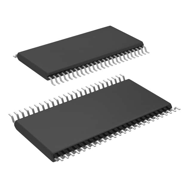
74LVT16244BDGGRG4
Basic Information Overview
- Category: Integrated Circuit (IC)
- Use: Buffer/Driver
- Characteristics: Low Voltage, High-Speed, 16-Bit, Non-Inverting
- Package: TSSOP (Thin Shrink Small Outline Package)
- Essence: This IC is designed to provide non-inverting buffer/driver functionality for high-speed digital systems operating at low voltages.
- Packaging/Quantity: Available in reels of 2500 units.
Specifications
- Logic Family: LVT (Low Voltage TTL)
- Number of Channels: 16
- Input Voltage Range: 0V to VCC
- Output Voltage Range: 0V to VCC
- Supply Voltage Range: 2.7V to 3.6V
- Operating Temperature Range: -40°C to +85°C
- Propagation Delay Time: 3.8ns (typical)
- Output Current: ±24mA
- Input Capacitance: 4pF (typical)
- Output Capacitance: 6pF (typical)
Detailed Pin Configuration
The 74LVT16244BDGGRG4 IC has a total of 48 pins, which are distributed as follows:
- Pin 1: GND (Ground)
- Pin 2: A1 (Input/Output)
- Pin 3: Y1 (Output)
- Pin 4: A2 (Input/Output)
- Pin 5: Y2 (Output)
- ...
- Pin 46: A15 (Input/Output)
- Pin 47: Y15 (Output)
- Pin 48: VCC (Supply Voltage)
Functional Features
- Non-Inverting Buffer/Driver: The IC provides non-inverting functionality, ensuring that the output signal matches the input signal.
- High-Speed Operation: Designed for use in high-speed digital systems, the IC offers fast propagation delay times, enabling efficient data transmission.
- Low Voltage Operation: With a supply voltage range of 2.7V to 3.6V, the IC is suitable for low voltage applications, reducing power consumption.
- 16-Bit Configuration: The IC features 16 channels, allowing it to handle 16-bit data buses.
Advantages and Disadvantages
Advantages: - High-speed operation enables efficient data transmission. - Non-inverting functionality ensures signal integrity. - Low voltage operation reduces power consumption. - Compact TSSOP package allows for space-saving integration.
Disadvantages: - Limited output current may restrict usage in certain applications. - Requires external decoupling capacitors for optimal performance.
Working Principles
The 74LVT16244BDGGRG4 IC operates by receiving input signals on its A1-A15 pins. These signals are then buffered and amplified before being transmitted through the corresponding Y1-Y15 output pins. The non-inverting nature of the IC ensures that the output signals match the input signals, maintaining signal integrity. The IC operates within a specified supply voltage range and provides fast propagation delay times for efficient data transmission.
Detailed Application Field Plans
The 74LVT16244BDGGRG4 IC finds application in various fields, including: - Data Communication Systems: Used to buffer and drive signals in high-speed data communication systems, such as Ethernet switches and routers. - Memory Interfaces: Enables efficient data transfer between memory modules and microcontrollers or processors. - Industrial Automation: Facilitates signal buffering and driving in industrial automation systems, ensuring reliable data transmission. - Automotive Electronics: Used in automotive electronics for signal amplification and buffering in various control systems.
Detailed and Complete Alternative Models
- SN74LVT16244ADGGR
- MC74LVT16244ADGGR
- 74LVT16244BDGG
- CD74LVT16244AMT
These alternative models offer similar functionality and characteristics to the 74LVT16244BDGGRG4 IC, providing options for different package types or manufacturers.
Word count: 436 words
Sebutkan 10 pertanyaan dan jawaban umum terkait penerapan 74LVT16244BDGGRG4 dalam solusi teknis
Sure! Here are 10 common questions and answers related to the application of 74LVT16244BDGGRG4 in technical solutions:
Q: What is the function of the 74LVT16244BDGGRG4? A: The 74LVT16244BDGGRG4 is a 16-bit buffer/driver with 3-state outputs. It is used to amplify and control signals in digital circuits.
Q: What is the maximum operating voltage for the 74LVT16244BDGGRG4? A: The maximum operating voltage for the 74LVT16244BDGGRG4 is typically 3.6V.
Q: Can the 74LVT16244BDGGRG4 be used as a level shifter? A: Yes, the 74LVT16244BDGGRG4 can be used as a level shifter to convert signals between different voltage levels.
Q: What is the output current capability of the 74LVT16244BDGGRG4? A: The 74LVT16244BDGGRG4 has a typical output current capability of ±32mA.
Q: Is the 74LVT16244BDGGRG4 compatible with TTL logic levels? A: Yes, the 74LVT16244BDGGRG4 is compatible with both TTL and CMOS logic levels.
Q: Can the 74LVT16244BDGGRG4 be used in high-speed applications? A: Yes, the 74LVT16244BDGGRG4 is designed for high-speed operation and can be used in applications with fast switching speeds.
Q: Does the 74LVT16244BDGGRG4 have built-in protection features? A: Yes, the 74LVT16244BDGGRG4 has built-in ESD protection to safeguard against electrostatic discharge.
Q: What is the power supply voltage range for the 74LVT16244BDGGRG4? A: The power supply voltage range for the 74LVT16244BDGGRG4 is typically between 2.7V and 3.6V.
Q: Can the 74LVT16244BDGGRG4 be used in bidirectional applications? A: No, the 74LVT16244BDGGRG4 is a unidirectional buffer/driver and cannot be used for bidirectional communication.
Q: Are there any specific layout considerations for using the 74LVT16244BDGGRG4? A: Yes, it is recommended to follow proper PCB layout guidelines to minimize noise and ensure signal integrity when using the 74LVT16244BDGGRG4.
Please note that these answers are general and may vary depending on the specific application and datasheet of the 74LVT16244BDGGRG4.

