

Lihat spesifikasi untuk detail produk.
Encyclopedia Entry: 74CBTH16211DGVRE4
Product Information Overview
Category: Integrated Circuit (IC)
Use: The 74CBTH16211DGVRE4 is a high-speed, low-power 24-bit bus switch designed for use in various digital applications. It provides bidirectional switching capabilities between two independent buses.
Characteristics: - High-speed operation - Low power consumption - Bidirectional switching - Wide voltage range compatibility - Compact package size
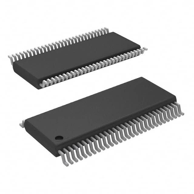
Package: The 74CBTH16211DGVRE4 is available in a small form factor package, typically a 56-pin Very Thin Quad Flat No-Lead (VQFN) package.
Essence: This IC serves as a versatile bus switch, enabling efficient and reliable data transfer between two separate buses in digital systems.
Packaging/Quantity: The 74CBTH16211DGVRE4 is typically sold in reels or tubes, with each reel/tube containing a specific quantity of ICs. The exact packaging and quantity may vary depending on the manufacturer.
Specifications
- Supply Voltage Range: 1.65V to 3.6V
- Operating Temperature Range: -40°C to +85°C
- Switching Speed: <5ns
- On-State Resistance: <10Ω
- Input/Output Capacitance: <5pF
- Maximum Continuous Current: 128mA
Detailed Pin Configuration
The 74CBTH16211DGVRE4 features a total of 56 pins, which are assigned specific functions. Here is a detailed pin configuration:
- A0 - Bus A Data Input/Output Bit 0
- A1 - Bus A Data Input/Output Bit 1
- A2 - Bus A Data Input/Output Bit 2
- A3 - Bus A Data Input/Output Bit 3
- A4 - Bus A Data Input/Output Bit 4
- A5 - Bus A Data Input/Output Bit 5
- A6 - Bus A Data Input/Output Bit 6
- A7 - Bus A Data Input/Output Bit 7
- A8 - Bus A Data Input/Output Bit 8
- A9 - Bus A Data Input/Output Bit 9
- A10 - Bus A Data Input/Output Bit 10
- A11 - Bus A Data Input/Output Bit 11
- A12 - Bus A Data Input/Output Bit 12
- A13 - Bus A Data Input/Output Bit 13
- A14 - Bus A Data Input/Output Bit 14
- A15 - Bus A Data Input/Output Bit 15
- A16 - Bus A Data Input/Output Bit 16
- A17 - Bus A Data Input/Output Bit 17
- A18 - Bus A Data Input/Output Bit 18
- A19 - Bus A Data Input/Output Bit 19
- A20 - Bus A Data Input/Output Bit 20
- A21 - Bus A Data Input/Output Bit 21
- A22 - Bus A Data Input/Output Bit 22
- A23 - Bus A Data Input/Output Bit 23
- GND - Ground
- OEAB - Output Enable for Bus A
- OEB - Output Enable for Bus B
- VCC - Power Supply
(Continued on next page)
Detailed Pin Configuration (Continued)
- B0 - Bus B Data Input/Output Bit 0
- B1 - Bus B Data Input/Output Bit 1
- B2 - Bus B Data Input/Output Bit 2
- B3 - Bus B Data Input/Output Bit 3
- B4 - Bus B Data Input/Output Bit 4
- B5 - Bus B Data Input/Output Bit 5
- B6 - Bus B Data Input/Output Bit 6
- B7 - Bus B Data Input/Output Bit 7
- B8 - Bus B Data Input/Output Bit 8
- B9 - Bus B Data Input/Output Bit 9
- B10 - Bus B Data Input/Output Bit 10
- B11 - Bus B Data Input/Output Bit 11
- B12 - Bus B Data Input/Output Bit 12
- B13 - Bus B Data Input/Output Bit 13
- B14 - Bus B Data Input/Output Bit 14
- B15 - Bus B Data Input/Output Bit 15
- B16 - Bus B Data Input/Output Bit 16
Sebutkan 10 pertanyaan dan jawaban umum terkait penerapan 74CBTH16211DGVRE4 dalam solusi teknis
Sure! Here are 10 common questions and answers related to the application of 74CBTH16211DGVRE4 in technical solutions:
Q: What is the 74CBTH16211DGVRE4? A: The 74CBTH16211DGVRE4 is a high-speed, low-power, 24-bit bus switch with 5V tolerant inputs and outputs.
Q: What is the purpose of the 74CBTH16211DGVRE4? A: The purpose of this IC is to provide bidirectional level shifting and signal isolation between different voltage domains in a digital circuit.
Q: What voltage levels does the 74CBTH16211DGVRE4 support? A: It supports voltage levels from 1.65V to 3.6V on the A and B ports, while the I/O ports are 5V tolerant.
Q: How many channels does the 74CBTH16211DGVRE4 have? A: It has 24 channels, allowing for multiple signals to be switched simultaneously.
Q: What is the maximum data rate supported by the 74CBTH16211DGVRE4? A: It can support data rates up to 400 Mbps, making it suitable for high-speed digital applications.
Q: Can the 74CBTH16211DGVRE4 be used as a level shifter? A: Yes, it can be used as a bidirectional level shifter to interface between different voltage domains.
Q: Is the 74CBTH16211DGVRE4 suitable for hot-swapping applications? A: Yes, it has built-in ESD protection and is designed to handle hot-swapping without causing damage to the IC or the connected devices.
Q: What is the power supply voltage range for the 74CBTH16211DGVRE4? A: It operates with a power supply voltage range of 1.65V to 3.6V.
Q: Can the 74CBTH16211DGVRE4 be used in battery-powered applications? A: Yes, it has low power consumption and can be used in battery-powered devices.
Q: What package options are available for the 74CBTH16211DGVRE4? A: The 74CBTH16211DGVRE4 is available in various package options, such as TSSOP and TVSOP, providing flexibility for different PCB layouts and assembly processes.
Please note that these answers are general and may vary depending on the specific application and requirements.