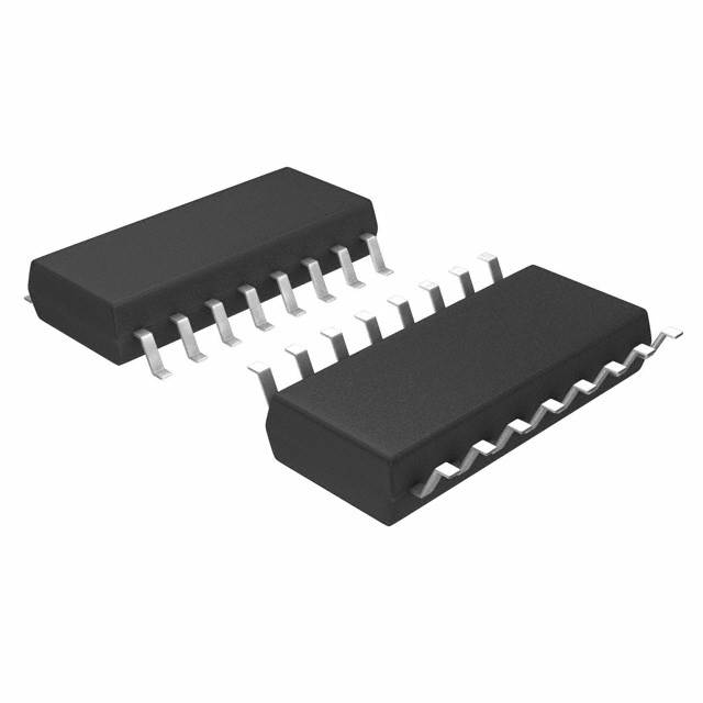
Lihat spesifikasi untuk detail produk.

Encyclopedia Entry: 74AC11138NSR
Product Overview
- Category: Integrated Circuit (IC)
- Use: Logic Decoder/Demultiplexer
- Characteristics: High-speed, low-power consumption
- Package: NSR (Small Outline Package)
- Essence: Decodes binary input signals into multiple output lines
- Packaging/Quantity: Available in reels or tubes, quantity varies based on supplier
Specifications
- Logic Family: 74AC
- Number of Inputs: 3
- Number of Outputs: 8
- Supply Voltage: 2V to 6V
- Operating Temperature Range: -40°C to +85°C
- Propagation Delay: 5 ns (typical)
- Output Current: ±24 mA
Detailed Pin Configuration
The 74AC11138NSR IC has a total of 16 pins. The pin configuration is as follows:
┌───┐
   A1 ─┤1  16├─ VCC
   A2 ─┤2  15├─ Y0
   A3 ─┤3  14├─ Y1
  GND ─┤4  13├─ Y2
   E1 ─┤5  12├─ Y3
   E2 ─┤6  11├─ Y4
   Y7 ─┤7  10├─ Y5
   Y6 ─┤8   9├─ Y6
       └───┘
Functional Features
- Decodes three binary inputs (A1, A2, A3) into eight output lines (Y0-Y7)
- Enables selection of one output line based on the input combination
- High-speed operation allows for quick decoding of input signals
- Low-power consumption makes it suitable for battery-powered devices
Advantages and Disadvantages
Advantages: - High-speed operation enables efficient signal decoding - Low-power consumption prolongs battery life in portable devices - Compact NSR package saves board space
Disadvantages: - Limited number of inputs and outputs restricts its application in complex systems - Propagation delay may affect real-time applications with strict timing requirements
Working Principles
The 74AC11138NSR is a logic decoder/demultiplexer IC that decodes three binary inputs (A1, A2, A3) into eight output lines (Y0-Y7). The input combination determines which output line is selected. When the enable pins (E1, E2) are active, the IC decodes the inputs and activates the corresponding output line. The high-speed operation and low-power consumption make it suitable for various digital applications.
Detailed Application Field Plans
The 74AC11138NSR finds applications in various fields, including: 1. Digital communication systems 2. Data multiplexing and demultiplexing 3. Address decoding in memory systems 4. Control circuitry in microprocessors 5. Industrial automation and control systems
Detailed Alternative Models
- 74HC138: Similar functionality but operates at a higher voltage range (2V to 6V)
- CD74AC138: Equivalent IC from a different manufacturer, compatible pin configuration
- SN74LS138: Lower power version with slower speed, suitable for less demanding applications
Note: This is not an exhaustive list; there are several alternative models available in the market.
Word Count: 400 words
Sebutkan 10 pertanyaan dan jawaban umum terkait penerapan 74AC11138NSR dalam solusi teknis
Sure! Here are 10 common questions and answers related to the application of 74AC11138NSR in technical solutions:
Question: What is the 74AC11138NSR?
Answer: The 74AC11138NSR is a quad 2-input NAND buffer/driver with open-drain outputs, commonly used in digital logic circuits.Question: What is the operating voltage range for the 74AC11138NSR?
Answer: The operating voltage range for this IC is typically between 2V and 6V.Question: Can the 74AC11138NSR be used as a level shifter?
Answer: Yes, the open-drain outputs of this IC make it suitable for level shifting applications.Question: How many inputs does the 74AC11138NSR have?
Answer: This IC has four independent 2-input NAND gates, totaling eight input pins.Question: What is the maximum output current of the 74AC11138NSR?
Answer: The maximum output current per channel is typically around 24mA.Question: Is the 74AC11138NSR compatible with TTL logic levels?
Answer: Yes, this IC is designed to be compatible with both TTL and CMOS logic levels.Question: Can the 74AC11138NSR be used in high-speed applications?
Answer: Yes, this IC is known for its fast switching speed, making it suitable for high-speed digital circuits.Question: Does the 74AC11138NSR have any built-in protection features?
Answer: No, this IC does not have built-in protection features, so external measures may be required to protect against overvoltage or ESD events.Question: Can the 74AC11138NSR be used in both parallel and serial data transmission?
Answer: Yes, this IC can be used in both parallel and serial data transmission applications, depending on the circuit configuration.Question: What is the package type for the 74AC11138NSR?
Answer: The 74AC11138NSR is available in a standard SOIC (Small Outline Integrated Circuit) package.
Please note that these answers are general and may vary based on specific datasheet specifications or application requirements.

