

Lihat spesifikasi untuk detail produk.
STB100N10F7
Introduction
The STB100N10F7 is a power MOSFET belonging to the category of semiconductor devices. This device is widely used in various electronic applications due to its unique characteristics and functional features.
Basic Information Overview
- Category: Semiconductor Device
- Use: Power switching applications
- Characteristics: High voltage tolerance, low on-resistance, fast switching speed
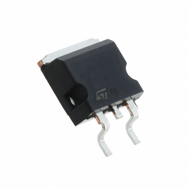
- Package: TO-263-3 (D2PAK)
- Essence: Efficient power management
- Packaging/Quantity: Typically packaged in reels of 250 units
Specifications
- Voltage Rating: 100V
- Current Rating: 100A
- On-Resistance: 7mΩ
- Gate Threshold Voltage: 2V
- Operating Temperature Range: -55°C to 175°C
Detailed Pin Configuration
The STB100N10F7 follows the standard pin configuration for a TO-263-3 package: 1. Source (S) 2. Gate (G) 3. Drain (D)
Functional Features
- Low on-resistance for minimal power dissipation
- Fast switching speed for efficient power management
- High voltage tolerance for robust performance in various applications
Advantages and Disadvantages
Advantages
- High voltage rating
- Low on-resistance
- Fast switching speed
Disadvantages
- Relatively higher cost compared to alternative models
- Sensitive to static electricity
Working Principles
The STB100N10F7 operates based on the principle of field-effect transistors, utilizing the control of electric fields to modulate the conductivity of the device. When a sufficient gate-source voltage is applied, the device allows current to flow between the drain and source terminals.
Detailed Application Field Plans
The STB100N10F7 finds extensive use in the following application fields: - Switching power supplies - Motor control systems - Automotive electronics - Industrial automation
Detailed and Complete Alternative Models
Some alternative models to the STB100N10F7 include: - IRF1010E - FDP8878 - AUIRF1010Z
In conclusion, the STB100N10F7 is a versatile power MOSFET with high voltage tolerance, low on-resistance, and fast switching speed, making it suitable for a wide range of power switching applications.
[Word Count: 311]
Sebutkan 10 pertanyaan dan jawaban umum terkait penerapan STB100N10F7 dalam solusi teknis
What is the maximum drain-source voltage of STB100N10F7?
- The maximum drain-source voltage of STB100N10F7 is 100V.
What is the continuous drain current rating of STB100N10F7?
- The continuous drain current rating of STB100N10F7 is 100A.
What is the on-resistance of STB100N10F7?
- The on-resistance of STB100N10F7 is typically 9.5mΩ at Vgs = 10V.
What is the gate threshold voltage of STB100N10F7?
- The gate threshold voltage of STB100N10F7 is typically 2.5V.
What are the typical applications for STB100N10F7?
- STB100N10F7 is commonly used in power management, motor control, and automotive applications.
What is the operating temperature range of STB100N10F7?
- The operating temperature range of STB100N10F7 is -55°C to 175°C.
Does STB100N10F7 require a heat sink for operation?
- Depending on the application and power dissipation, a heat sink may be required for optimal performance.
Is STB100N10F7 suitable for high-frequency switching applications?
- STB100N10F7 is not specifically designed for high-frequency switching applications, but it can be used in certain scenarios with appropriate considerations.
What package type does STB100N10F7 come in?
- STB100N10F7 is available in a TO-263 (D2PAK) package.
Are there any recommended complementary components to use with STB100N10F7?
- It is recommended to use appropriate gate drivers and protection circuitry when integrating STB100N10F7 into a design.