Lihat spesifikasi untuk detail produk.

M74HCT652B1R
Product Overview
Category
M74HCT652B1R belongs to the category of integrated circuits (ICs).
Use
This IC is commonly used for data bus multiplexing and demultiplexing applications.
Characteristics
- High-speed operation
- Wide operating voltage range
- Low power consumption
- Schmitt trigger inputs for noise immunity
- TTL compatibility
- 3-state outputs for bus-oriented applications
Package
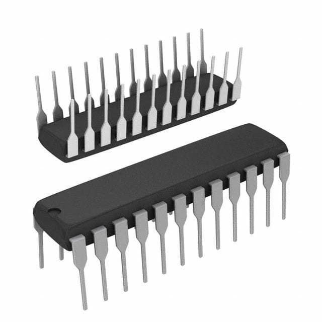
The M74HCT652B1R is available in a standard 24-pin SOIC (Small Outline Integrated Circuit) package.
Essence
The essence of M74HCT652B1R lies in its ability to efficiently multiplex and demultiplex data buses, enabling effective communication between multiple devices.
Packaging/Quantity
The M74HCT652B1R is typically packaged in reels containing 2500 units.
Specifications
- Supply Voltage Range: 4.5V to 5.5V
- Input Voltage Range: 0V to VCC
- Output Voltage Range: 0V to VCC
- Operating Temperature Range: -40°C to +125°C
- Maximum Propagation Delay Time: 25ns
- Maximum Quiescent Current: 8µA
Detailed Pin Configuration
The M74HCT652B1R has a total of 24 pins, which are assigned specific functions as follows:
- A1: Data Bus A, Bit 1
- B1: Data Bus B, Bit 1
- GND: Ground
- A2: Data Bus A, Bit 2
- B2: Data Bus B, Bit 2
- A3: Data Bus A, Bit 3
- B3: Data Bus B, Bit 3
- A4: Data Bus A, Bit 4
- B4: Data Bus B, Bit 4
- A5: Data Bus A, Bit 5
- B5: Data Bus B, Bit 5
- A6: Data Bus A, Bit 6
- B6: Data Bus B, Bit 6
- A7: Data Bus A, Bit 7
- B7: Data Bus B, Bit 7
- A8: Data Bus A, Bit 8
- B8: Data Bus B, Bit 8
- OE: Output Enable
- DIR: Direction Control
- VCC: Supply Voltage
- Y1: Multiplexed Output 1
- Y2: Multiplexed Output 2
- GND: Ground
- Y3: Multiplexed Output 3
Functional Features
- Bidirectional data bus multiplexing and demultiplexing
- 3-state outputs for bus-oriented applications
- Schmitt trigger inputs for improved noise immunity
- TTL compatibility for easy integration with existing systems
Advantages and Disadvantages
Advantages
- High-speed operation allows for efficient data transfer
- Wide operating voltage range ensures compatibility with various systems
- Low power consumption helps conserve energy
- Schmitt trigger inputs provide robustness against noise
- 3-state outputs enable bus-oriented applications
Disadvantages
- Limited number of multiplexed outputs (3 in total)
- May require additional components for complex data bus configurations
Working Principles
The M74HCT652B1R operates by receiving input data from two separate buses, A and B. The direction control pin (DIR) determines whether the IC functions as a multiplexer or a demultiplexer. When operating as a multiplexer, the IC selects and outputs data from either bus A or B based on the control signal. In demultiplexer mode, the IC routes the input data to the appropriate output bus based on the control signal. The output enable pin (OE) enables or disables the outputs.
Detailed Application Field Plans
The M74HCT652B1R finds applications in various fields, including:
- Data communication systems
- Microprocessor-based systems
- Industrial automation
- Automotive electronics
- Telecommunications equipment
Detailed and Complete Alternative Models
- SN74HCT652N: Similar functionality and specifications, available in a DIP (Dual Inline Package) format.
- CD74HCT652E: Equivalent IC with identical features, offered in a PDIP (Plastic Dual Inline Package) package.
- 74HC652: Alternative IC with similar functionality, but operates at a higher voltage range.
These alternative models can be considered based on specific requirements and compatibility with existing systems.
Word count: 529 words
Sebutkan 10 pertanyaan dan jawaban umum terkait penerapan M74HCT652B1R dalam solusi teknis
Sure! Here are 10 common questions and answers related to the application of M74HCT652B1R in technical solutions:
Q1: What is the M74HCT652B1R? A1: The M74HCT652B1R is a high-speed CMOS octal bus transceiver with three-state outputs. It can be used for bidirectional data transfer between different voltage systems.
Q2: What is the operating voltage range of the M74HCT652B1R? A2: The M74HCT652B1R operates within a voltage range of 4.5V to 5.5V.
Q3: How many bidirectional channels does the M74HCT652B1R have? A3: The M74HCT652B1R has 8 bidirectional channels, allowing for simultaneous data transfer in both directions.
Q4: Can the M74HCT652B1R handle different voltage levels on its inputs and outputs? A4: Yes, the M74HCT652B1R is designed to handle different voltage levels on its inputs and outputs, making it suitable for interfacing between systems with different voltage requirements.
Q5: What is the maximum data transfer rate supported by the M74HCT652B1R? A5: The M74HCT652B1R supports high-speed data transfer rates up to 25 MHz.
Q6: Does the M74HCT652B1R have internal pull-up or pull-down resistors? A6: No, the M74HCT652B1R does not have internal pull-up or pull-down resistors. External resistors may be required for proper operation.
Q7: Can the M74HCT652B1R be used in applications requiring hot-swapping of devices? A7: Yes, the M74HCT652B1R supports hot-swapping, allowing for the insertion and removal of devices without disrupting the operation of the system.
Q8: What is the power consumption of the M74HCT652B1R? A8: The power consumption of the M74HCT652B1R depends on various factors such as operating frequency and load conditions. Please refer to the datasheet for detailed information.
Q9: Can the M74HCT652B1R be used in automotive applications? A9: Yes, the M74HCT652B1R is suitable for automotive applications as it meets the necessary requirements for automotive electronics.
Q10: Are there any special considerations for PCB layout when using the M74HCT652B1R? A10: Yes, proper PCB layout techniques should be followed to minimize noise, ensure signal integrity, and optimize performance. The datasheet provides guidelines for PCB layout and design considerations.
Please note that these answers are general and may vary depending on specific application requirements. It is always recommended to consult the datasheet and relevant technical documentation for accurate and detailed information.

