

Lihat spesifikasi untuk detail produk.
Encyclopedia Entry: 74V1G125CTR
Product Information Overview
- Category: Integrated Circuit (IC)
- Use: Buffer/Driver
- Characteristics: High-speed, low-power, single gate, non-inverting buffer/driver
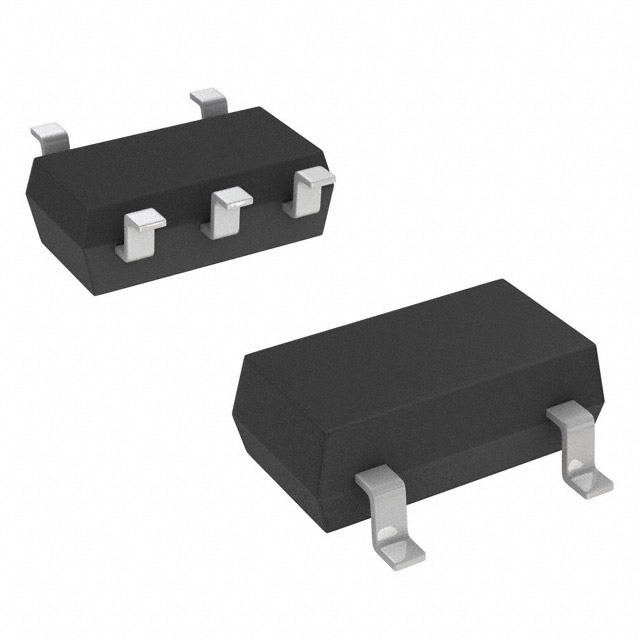
- Package: SOT-23-5
- Essence: The 74V1G125CTR is a versatile IC that provides buffering and driving capabilities for digital signals.
- Packaging/Quantity: Available in tape and reel packaging with 3000 units per reel.
Specifications
- Supply Voltage: 1.65V to 5.5V
- Input Voltage: 0V to VCC
- Output Voltage: 0V to VCC
- Operating Temperature Range: -40°C to +85°C
- Propagation Delay: 3.8ns (typical) at 3.3V supply voltage
- Output Current: ±8mA
- Input Capacitance: 2pF (typical)
Detailed Pin Configuration
The 74V1G125CTR has a total of 5 pins arranged as follows:
____
   Y ---|    |
   A ---|    |
   GND -|    |
   B ---|    |
   VCC -|____|
- Pin 1 (Y): Output pin, connected to the output signal.
- Pin 2 (A): Input pin, receives the input signal.
- Pin 3 (GND): Ground pin, connected to the ground reference.
- Pin 4 (B): Input pin, receives the input signal.
- Pin 5 (VCC): Power supply pin, connected to the positive supply voltage.
Functional Features
- Non-inverting buffer/driver: The 74V1G125CTR amplifies and buffers digital signals without changing their logic levels.
- High-speed operation: With a propagation delay of only 3.8ns, it ensures fast signal transmission.
- Low-power consumption: Designed to operate efficiently with a supply voltage range of 1.65V to 5.5V.
- Wide operating temperature range: Can function reliably in temperatures ranging from -40°C to +85°C.
Advantages and Disadvantages
Advantages: - Compact package size (SOT-23-5) allows for space-efficient designs. - Versatile IC suitable for various digital signal buffering and driving applications. - High-speed operation enables efficient data transmission.
Disadvantages: - Limited output current capability compared to some other buffer/driver ICs. - Not suitable for high-voltage applications due to the limited supply voltage range.
Working Principles
The 74V1G125CTR operates as a non-inverting buffer/driver. It receives digital input signals on pins A and B and amplifies them to the same logic level at the output pin Y. The IC is designed to provide high-speed signal buffering while consuming low power. It operates within a specified supply voltage range and can withstand a wide temperature range.
Detailed Application Field Plans
The 74V1G125CTR finds applications in various fields where digital signal buffering and driving are required. Some potential application areas include:
- Communication Systems: Used in signal amplification and buffering stages of communication devices such as routers, switches, and modems.
- Industrial Automation: Employed in control systems to amplify and drive digital signals between sensors, actuators, and programmable logic controllers (PLCs).
- Consumer Electronics: Integrated into audio/video equipment, gaming consoles, and home automation systems to enhance signal quality and ensure reliable data transmission.
- Automotive Electronics: Utilized in automotive control units, infotainment systems, and driver assistance modules for signal buffering and driving purposes.
Detailed and Complete Alternative Models
- 74LVC1G125: Similar non-inverting buffer/driver IC with a wider supply voltage range (1.65V to 5.5V) and higher output current capability.
- SN74LVC1G125DBVR: Non-inverting buffer/driver IC in SOT-23-5 package with comparable specifications and performance.
- MC74VHCT125ADR2G: Buffer/driver IC with tri-state outputs, suitable for bus-oriented applications.
(Note: This list is not exhaustive and other alternative models may exist.)
Word Count: 464 words
Sebutkan 10 pertanyaan dan jawaban umum terkait penerapan 74V1G125CTR dalam solusi teknis
Sure! Here are 10 common questions and answers related to the application of 74V1G125CTR in technical solutions:
Q: What is the function of the 74V1G125CTR? A: The 74V1G125CTR is a single bus buffer gate with three-state output, used for signal buffering and level shifting.
Q: What is the voltage range supported by the 74V1G125CTR? A: The 74V1G125CTR supports a wide voltage range from 1.65V to 5.5V.
Q: Can the 74V1G125CTR be used for bidirectional communication? A: No, the 74V1G125CTR is a unidirectional buffer gate and cannot be used for bidirectional communication.
Q: How many inputs does the 74V1G125CTR have? A: The 74V1G125CTR has one input pin.
Q: How many outputs does the 74V1G125CTR have? A: The 74V1G125CTR has one output pin.
Q: What is the maximum output current of the 74V1G125CTR? A: The 74V1G125CTR can provide a maximum output current of 32mA.
Q: Can the 74V1G125CTR be used in high-speed applications? A: Yes, the 74V1G125CTR is designed for high-speed operation and can be used in such applications.
Q: Is the 74V1G125CTR compatible with other logic families? A: Yes, the 74V1G125CTR is compatible with various logic families, including TTL, CMOS, and LVCMOS.
Q: Can the 74V1G125CTR be used in automotive applications? A: Yes, the 74V1G125CTR is suitable for automotive applications as it meets the necessary standards and specifications.
Q: What is the package type of the 74V1G125CTR? A: The 74V1G125CTR is available in a small SOT-23 package, which is commonly used for surface mount applications.
Please note that these answers are general and may vary depending on the specific datasheet and application requirements.