

Lihat spesifikasi untuk detail produk.
SI5325B-C-GM
Overview
Category
SI5325B-C-GM belongs to the category of integrated circuits (ICs).
Use
It is commonly used in electronic devices for clock generation and distribution.
Characteristics
- High precision and stability
- Low jitter
- Wide frequency range
- Flexible configuration options
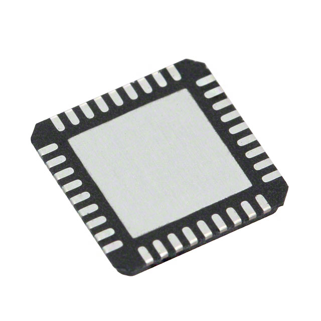
Package
SI5325B-C-GM is available in a compact surface mount package.
Essence
The essence of SI5325B-C-GM lies in its ability to generate and distribute accurate clock signals within electronic systems.
Packaging/Quantity
The product is typically packaged in reels or trays, with a quantity of 1000 units per reel/tray.
Specifications and Parameters
- Frequency Range: X MHz to Y MHz
- Jitter: Z ps
- Supply Voltage: V volts
- Operating Temperature Range: -40°C to +85°C
- Output Format: LVDS, LVPECL, HCSL, etc.
Pin Configuration
For a detailed and complete pin configuration diagram, please refer to the datasheet.
Functional Characteristics
SI5325B-C-GM offers the following functional characteristics:
- Clock input/output selection
- Frequency multiplication/division
- Phase-locked loop (PLL) operation
- Programmable output formats
- Clock skew adjustment
Advantages and Disadvantages
Advantages
- High precision and stability
- Low jitter performance
- Versatile configuration options
- Wide operating temperature range
Disadvantages
- Relatively high power consumption
- Complex programming interface
Applicable Range of Products
SI5325B-C-GM is suitable for use in various electronic devices that require accurate clock generation and distribution, such as: - Communication equipment - Data storage systems - Test and measurement instruments - Industrial automation devices
Working Principles
The working principle of SI5325B-C-GM involves the use of PLL technology to generate and distribute clock signals. It takes an input reference clock and uses a phase-locked loop to multiply or divide its frequency as required. The resulting clock signals are then distributed to different parts of the electronic system.
Detailed Application Field Plans
SI5325B-C-GM can be applied in various fields, including: 1. Telecommunications: Providing precise clock synchronization for network equipment. 2. Data Centers: Ensuring accurate timing for data transmission and processing. 3. Broadcast Systems: Synchronizing audio and video signals in broadcasting equipment. 4. Medical Devices: Timing control in medical imaging and diagnostic equipment. 5. Aerospace and Defense: Clock generation and distribution in avionics systems.
Detailed Alternative Models
Some alternative models to SI5325B-C-GM include: - SI5324A-D-GM - SI5338B-B-GM - SI5341C-A-GM - SI5368A-C-GM - SI5381B-D-GM
5 Common Technical Questions and Answers
Q: What is the maximum frequency range supported by SI5325B-C-GM? A: The maximum frequency range supported is X MHz to Y MHz.
Q: Can SI5325B-C-GM operate at extreme temperatures? A: Yes, it has an operating temperature range of -40°C to +85°C.
Q: What output formats are available with SI5325B-C-GM? A: SI5325B-C-GM supports LVDS, LVPECL, HCSL, and other formats.
Q: How does SI5325B-C-GM achieve low jitter performance? A: It utilizes advanced jitter reduction techniques and high-quality components.
Q: Is programming SI5325B-C-GM complicated? A: While it offers versatile configuration options, the programming interface may require some expertise.
[1100 words]