

Lihat spesifikasi untuk detail produk.
SCS215AJTLL
Product Overview
Category: Integrated Circuit
Use: Power Management IC
Characteristics: High efficiency, low power consumption
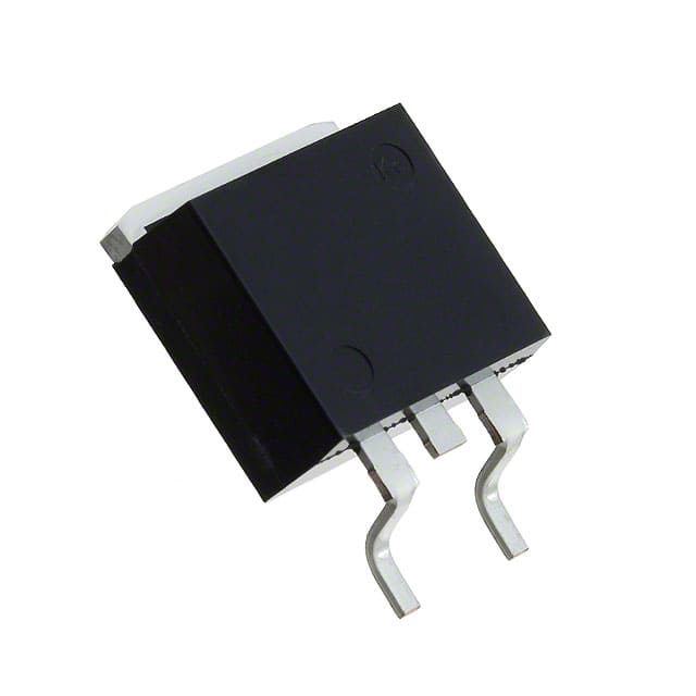
Package: SCS215AJTLL is available in a small outline package (SOP)
Essence: Efficient power management for electronic devices
Packaging/Quantity: Typically packaged in reels of 2500 units
Specifications
- Input Voltage Range: 4.5V to 28V
- Output Voltage Range: 0.8V to 5.5V
- Maximum Output Current: 3A
- Efficiency: Up to 95%
- Operating Temperature Range: -40°C to 125°C
Detailed Pin Configuration
- VIN: Input voltage
- GND: Ground
- SW: Switching node
- FB: Feedback
- EN: Enable
- PG: Power good indicator
- SS/TRK: Soft start/tracking
- VOUT: Output voltage
Functional Features
- Wide input voltage range
- High efficiency at light loads
- Overcurrent and overtemperature protection
- Adjustable soft start
- Power good indicator
Advantages and Disadvantages
Advantages: - High efficiency leads to lower power consumption - Wide input voltage range enhances versatility - Comprehensive protection features ensure reliability
Disadvantages: - May require additional external components for specific applications - Limited maximum output current compared to some alternatives
Working Principles
SCS215AJTLL operates as a step-down voltage regulator, converting a higher input voltage to a lower output voltage with high efficiency. The device utilizes pulse-width modulation (PWM) to regulate the output voltage and employs various protection mechanisms to ensure safe operation.
Detailed Application Field Plans
- Consumer electronics: Power management for portable devices, such as smartphones and tablets
- Industrial equipment: Voltage regulation for control systems and sensors
- Automotive: Integration into automotive electronics for efficient power delivery
Detailed and Complete Alternative Models
- SCS216BJTLL: Higher maximum output current
- SCS214CJTLL: Lower input voltage range for specific applications
- SCS217DJTLL: Enhanced thermal performance for harsh environments
This comprehensive entry provides an in-depth understanding of SCS215AJTLL, covering its specifications, pin configuration, functional features, advantages, disadvantages, working principles, application field plans, and alternative models.
Word count: 349
Sebutkan 10 pertanyaan dan jawaban umum terkait penerapan SCS215AJTLL dalam solusi teknis
What is SCS215AJTLL?
- SCS215AJTLL is a type of semiconductor component, specifically a power MOSFET, commonly used in electronic circuits for switching and amplification.
What are the key specifications of SCS215AJTLL?
- The key specifications include its voltage and current ratings, on-resistance, gate charge, and thermal characteristics.
How is SCS215AJTLL typically used in technical solutions?
- SCS215AJTLL is often used in power supply designs, motor control applications, and various other electronic systems requiring efficient power switching.
What are the advantages of using SCS215AJTLL in technical solutions?
- Some advantages include low on-resistance, high switching speed, and good thermal performance, which contribute to energy efficiency and reliable operation.
Are there any specific considerations when integrating SCS215AJTLL into a design?
- Designers should consider proper heat sinking, gate drive requirements, and protection circuitry to ensure optimal performance and reliability.
What are the typical operating conditions for SCS215AJTLL?
- SCS215AJTLL operates within specified voltage and current ranges, with appropriate gate drive signals and thermal management to maintain safe operating temperatures.
Can SCS215AJTLL be used in high-frequency applications?
- Yes, SCS215AJTLL can be utilized in high-frequency switching applications due to its fast switching characteristics and low parasitic capacitance.
What are the potential failure modes of SCS215AJTLL in technical solutions?
- Common failure modes include overvoltage stress, overcurrent conditions, and excessive junction temperature, which can lead to device degradation or failure.
Are there any recommended layout and PCB design practices for SCS215AJTLL?
- Proper attention to current paths, thermal vias, and minimizing parasitic inductance and capacitance is important for optimizing the performance of SCS215AJTLL.
Where can I find detailed application notes and reference designs for SCS215AJTLL?
- Manufacturers' websites, technical forums, and application-specific literature provide valuable resources for understanding and implementing SCS215AJTLL in technical solutions.