Lihat spesifikasi untuk detail produk.

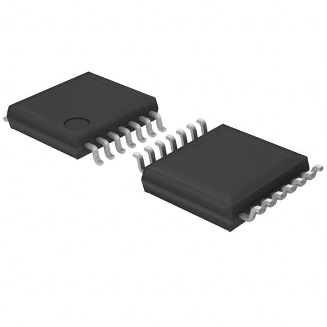
BU4066BCFV-E2
Product Overview
- Category: Integrated Circuit (IC)
- Use: Digital Switch
- Characteristics:
- Quad bilateral switch
- Low power consumption
- Wide operating voltage range
- High noise immunity
- Package: TSSOP-14
- Essence: The BU4066BCFV-E2 is a quad bilateral switch IC used for digital signal switching applications.
- Packaging/Quantity: Available in tape and reel packaging, with 2500 units per reel.
Specifications
- Supply Voltage Range: 3V to 15V
- On-state Resistance: 125Ω (typical)
- Operating Temperature Range: -40°C to +85°C
- Input Capacitance: 5pF (typical)
- Propagation Delay Time: 200ns (typical)
Detailed Pin Configuration
The BU4066BCFV-E2 has a TSSOP-14 package with the following pin configuration:
____
   1 |      | 14
   2 |      | 13
   3 |      | 12
   4 |      | 11
   5 |      | 10
   6 |      | 9
   7 |______| 8
Functional Features
- Four independent bilateral switches
- Each switch can be independently controlled
- Low "ON" resistance for minimal signal distortion
- High noise immunity for reliable operation
- Wide operating voltage range allows compatibility with various systems
Advantages and Disadvantages
Advantages: - Low power consumption - Compact size - Easy to use and integrate into circuits - High reliability and durability
Disadvantages: - Limited number of switches (4) - Not suitable for high-frequency applications
Working Principles
The BU4066BCFV-E2 operates based on the principle of a bilateral switch. It consists of four independent switches that can be controlled by applying appropriate control signals to the input pins. When the control signal is high, the corresponding switch turns "ON," allowing the passage of digital signals. Conversely, when the control signal is low, the switch turns "OFF," blocking the signal.
Detailed Application Field Plans
The BU4066BCFV-E2 finds applications in various fields, including:
Audio and Video Signal Routing: The quad bilateral switch can be used to route audio and video signals in multimedia systems, allowing users to switch between different sources or destinations.
Communication Systems: The IC can be utilized in communication systems for signal switching, enabling the selection of different channels or modes.
Test and Measurement Equipment: The switch's low distortion and wide operating voltage range make it suitable for use in test and measurement equipment, such as oscilloscopes and data loggers.
Industrial Control Systems: The BU4066BCFV-E2 can be employed in industrial control systems for signal routing and switching tasks, facilitating automation and process control.
Detailed and Complete Alternative Models
- CD4066BCN: Quad bilateral switch with similar specifications and pin configuration, available in DIP-14 package.
- TS5A3160DBVR: Analog switch with similar characteristics, available in SOT-23-5 package.
- MAX4617CSE+: High-performance analog switch with enhanced features, available in SOIC-16 package.
These alternative models offer similar functionality and can be considered as substitutes for the BU4066BCFV-E2 depending on specific requirements.
Word count: 431 words
Sebutkan 10 pertanyaan dan jawaban umum terkait penerapan BU4066BCFV-E2 dalam solusi teknis
Sure! Here are 10 common questions and answers related to the application of BU4066BCFV-E2 in technical solutions:
Question: What is BU4066BCFV-E2?
Answer: BU4066BCFV-E2 is a quad bilateral switch IC that can be used for analog signal switching applications.Question: What is the maximum voltage rating of BU4066BCFV-E2?
Answer: The maximum voltage rating of BU4066BCFV-E2 is typically around 20V.Question: Can BU4066BCFV-E2 be used for digital signal switching as well?
Answer: Yes, BU4066BCFV-E2 can be used for both analog and digital signal switching applications.Question: What is the typical on-resistance of each switch in BU4066BCFV-E2?
Answer: The typical on-resistance of each switch in BU4066BCFV-E2 is around 100 ohms.Question: What is the maximum current handling capability of BU4066BCFV-E2?
Answer: The maximum current handling capability of BU4066BCFV-E2 is typically around 25mA.Question: Can BU4066BCFV-E2 be used for audio signal switching?
Answer: Yes, BU4066BCFV-E2 can be used for audio signal switching applications due to its low distortion characteristics.Question: Is BU4066BCFV-E2 suitable for high-frequency signal switching?
Answer: BU4066BCFV-E2 has a relatively low bandwidth, so it may not be suitable for high-frequency signal switching above a few MHz.Question: Can BU4066BCFV-E2 be used in battery-powered applications?
Answer: Yes, BU4066BCFV-E2 has a low power consumption and can be used in battery-powered applications.Question: Does BU4066BCFV-E2 have built-in protection features?
Answer: No, BU4066BCFV-E2 does not have built-in protection features, so external protection circuitry may be required.Question: What is the package type of BU4066BCFV-E2?
Answer: BU4066BCFV-E2 is available in a small surface-mount package called SOP-14.
Please note that the answers provided here are general and may vary depending on specific datasheet specifications and application requirements.

