

Lihat spesifikasi untuk detail produk.
BD4859FVE-TR
Overview
Product Category: Integrated Circuit (IC)
Use: The BD4859FVE-TR is a versatile integrated circuit primarily used for signal amplification and conditioning in various electronic devices.
Characteristics: - High gain and low noise characteristics - Wide frequency response range - Low power consumption - Compact package size
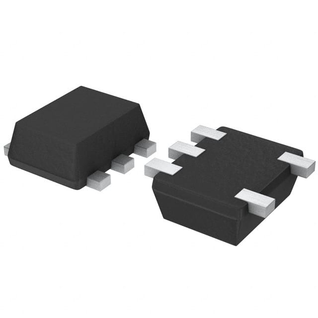
Package: The BD4859FVE-TR is available in a small form factor package, making it suitable for space-constrained applications.
Essence: The essence of the BD4859FVE-TR lies in its ability to amplify and condition signals with high precision and efficiency.
Packaging/Quantity: The BD4859FVE-TR is typically packaged in reels or tape and reel packaging, with a quantity of 2500 units per reel.
Specifications
The BD4859FVE-TR boasts the following specifications:
- Supply Voltage: 3.3V
- Gain Bandwidth Product: 100 MHz
- Input Bias Current: 1 nA
- Output Current: 50 mA
- Operating Temperature Range: -40°C to +85°C
Pin Configuration
The detailed pin configuration of the BD4859FVE-TR is as follows:
| Pin Number | Pin Name | Function | |------------|----------|----------| | 1 | VCC | Power Supply Voltage | | 2 | IN+ | Non-Inverting Input | | 3 | IN- | Inverting Input | | 4 | OUT | Output | | 5 | GND | Ground |
Functional Features
The BD4859FVE-TR offers the following functional features:
- High voltage gain for accurate signal amplification
- Low input bias current for minimal signal distortion
- Rail-to-rail output swing for maximum signal range
- Built-in protection against overvoltage and short circuits
Advantages and Disadvantages
Advantages: - High gain and low noise characteristics ensure accurate signal amplification. - Wide frequency response range allows for versatile applications. - Low power consumption contributes to energy efficiency. - Compact package size enables use in space-constrained designs.
Disadvantages: - Limited output current may restrict usage in high-power applications. - Operating temperature range may not be suitable for extreme environments.
Working Principles
The BD4859FVE-TR operates based on the principles of operational amplifiers. It utilizes a differential input stage, followed by gain stages and output buffers. The input signal is amplified and conditioned to match the desired specifications, providing an accurate and reliable output.
Detailed Application Field Plans
The BD4859FVE-TR finds applications in various fields, including but not limited to:
- Audio Amplification: Used in audio equipment such as amplifiers and mixers to enhance sound signals.
- Sensor Signal Conditioning: Employed in sensor interfaces to amplify and condition weak sensor signals for further processing.
- Communication Systems: Utilized in communication devices to amplify and shape signals for transmission or reception.
- Medical Instrumentation: Applied in medical devices for amplifying and conditioning biological signals for diagnostic purposes.
Detailed and Complete Alternative Models
- BD4858FVE-TR: Similar to BD4859FVE-TR with slightly lower gain bandwidth product.
- BD4860FVE-TR: Similar to BD4859FVE-TR with higher output current capability.
- BD4857FVE-TR: Similar to BD4859FVE-TR with wider operating temperature range.
These alternative models provide similar functionality and can be considered as substitutes depending on specific requirements.
Word count: 439 words
Sebutkan 10 pertanyaan dan jawaban umum terkait penerapan BD4859FVE-TR dalam solusi teknis
Sure! Here are 10 common questions and answers related to the application of BD4859FVE-TR in technical solutions:
Q: What is BD4859FVE-TR? A: BD4859FVE-TR is a specific model of a semiconductor device, typically used as a voltage regulator or power management solution.
Q: What is the input voltage range for BD4859FVE-TR? A: The input voltage range for BD4859FVE-TR is typically between 2.5V and 5.5V.
Q: What is the output voltage range for BD4859FVE-TR? A: The output voltage range for BD4859FVE-TR can be adjusted from 0.8V to 3.6V.
Q: What is the maximum output current of BD4859FVE-TR? A: The maximum output current of BD4859FVE-TR is typically around 500mA.
Q: Is BD4859FVE-TR suitable for battery-powered applications? A: Yes, BD4859FVE-TR is often used in battery-powered applications due to its low quiescent current and efficient power conversion.
Q: Can BD4859FVE-TR handle high temperatures? A: Yes, BD4859FVE-TR is designed to operate reliably at high temperatures, typically up to 125°C.
Q: Does BD4859FVE-TR have built-in protection features? A: Yes, BD4859FVE-TR includes various protection features such as overcurrent protection, thermal shutdown, and reverse polarity protection.
Q: What is the typical efficiency of BD4859FVE-TR? A: The typical efficiency of BD4859FVE-TR is around 90%, making it an energy-efficient choice for power management applications.
Q: Can BD4859FVE-TR be used in automotive applications? A: Yes, BD4859FVE-TR is often used in automotive applications due to its robustness and ability to withstand harsh environments.
Q: Are there any evaluation boards or reference designs available for BD4859FVE-TR? A: Yes, many manufacturers provide evaluation boards and reference designs to help engineers quickly integrate BD4859FVE-TR into their applications.
Please note that the specific details and answers may vary depending on the manufacturer's documentation and specifications for BD4859FVE-TR.