

Lihat spesifikasi untuk detail produk.
NC7SV74L8X
Product Overview
- Category: Integrated Circuit (IC)
- Use: Flip-Flop
- Characteristics: Low-power, Single D-Type Positive-Edge-Triggered Flip-Flop
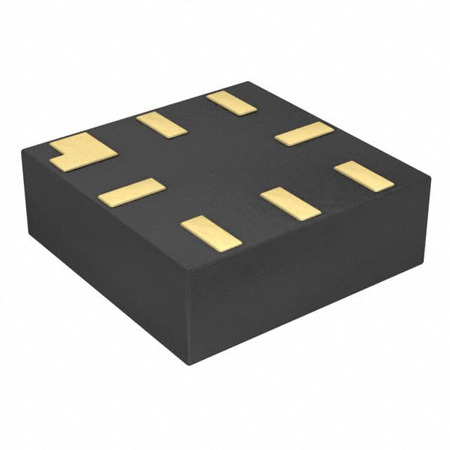
- Package: 8-Lead MicroPak™
- Essence: This IC is designed to store a single bit of data and is commonly used in digital circuits for sequential logic operations.
- Packaging/Quantity: Available in tape and reel packaging with a quantity of 3000 units per reel.
Specifications
- Supply Voltage Range: 1.65V to 5.5V
- Operating Temperature Range: -40°C to +85°C
- Input Voltage High: 0.7 x VCC
- Input Voltage Low: 0.3 x VCC
- Output Voltage High: VCC - 0.4V
- Output Voltage Low: 0.4V
Detailed Pin Configuration
The NC7SV74L8X has the following pin configuration:
- CLK (Clock Input)
- D (Data Input)
- Q (Flip-Flop Output)
- GND (Ground)
- Q̅ (Complementary Output)
- PRE (Preset Input)
- CLR (Clear Input)
- VCC (Supply Voltage)
Functional Features
- Positive-edge-triggered flip-flop with asynchronous preset and clear inputs.
- Low-power consumption makes it suitable for battery-powered devices.
- Wide supply voltage range allows compatibility with various systems.
- Compact 8-Lead MicroPak™ package saves board space.
Advantages and Disadvantages
Advantages: - Low power consumption - Wide supply voltage range - Compact package size
Disadvantages: - Limited number of flip-flops in a single package - Lack of additional advanced features
Working Principles
The NC7SV74L8X is a positive-edge-triggered flip-flop, which means it captures the input data (D) and updates the output (Q) only when a rising edge is detected on the clock input (CLK). The asynchronous preset (PRE) and clear (CLR) inputs allow for immediate control over the output state. The IC operates within a specified supply voltage range and provides reliable logic level conversions.
Detailed Application Field Plans
The NC7SV74L8X can be used in various digital systems and applications, including but not limited to:
- Microcontrollers and microprocessors
- Communication devices
- Data storage systems
- Consumer electronics
- Industrial automation
Detailed and Complete Alternative Models
- SN74LVC1G74 - Single D-Type Flip-Flop with Preset and Clear
- CD4013B - Dual D-Type Flip-Flop
- MC74HC74A - Dual D-Type Flip-Flop with Set and Reset
These alternative models offer similar functionality and can be considered as substitutes for the NC7SV74L8X depending on specific requirements and design constraints.
Word count: 311 words
Sebutkan 10 pertanyaan dan jawaban umum terkait penerapan NC7SV74L8X dalam solusi teknis
Sure! Here are 10 common questions and answers related to the application of NC7SV74L8X in technical solutions:
Question: What is NC7SV74L8X?
- Answer: NC7SV74L8X is a specific model of a dual D-type flip-flop integrated circuit (IC) that is commonly used in digital logic applications.Question: What is the purpose of using NC7SV74L8X in technical solutions?
- Answer: The NC7SV74L8X IC is used to store and manipulate binary data in digital circuits, making it suitable for various applications such as data storage, synchronization, and signal processing.Question: What voltage levels does NC7SV74L8X support?
- Answer: NC7SV74L8X supports a wide range of voltage levels, typically ranging from 1.65V to 5.5V, making it compatible with various power supply systems.Question: Can NC7SV74L8X be used in battery-powered devices?
- Answer: Yes, NC7SV74L8X can be used in battery-powered devices as it operates at low power consumption levels, making it suitable for portable and energy-efficient applications.Question: How many flip-flops are there in NC7SV74L8X?
- Answer: NC7SV74L8X consists of two independent D-type flip-flops, allowing for simultaneous or sequential data storage and manipulation.Question: What is the maximum clock frequency supported by NC7SV74L8X?
- Answer: The maximum clock frequency supported by NC7SV74L8X is typically around 200 MHz, enabling high-speed data processing in digital circuits.Question: Can NC7SV74L8X be cascaded to create larger storage systems?
- Answer: Yes, multiple NC7SV74L8X ICs can be cascaded together to create larger storage systems by connecting the output of one flip-flop to the input of another.Question: Is NC7SV74L8X compatible with other digital logic families?
- Answer: Yes, NC7SV74L8X is designed to be compatible with various digital logic families, such as CMOS and TTL, allowing for seamless integration with existing circuitry.Question: What are the typical operating temperature ranges for NC7SV74L8X?
- Answer: NC7SV74L8X typically operates within a temperature range of -40°C to 85°C, making it suitable for both commercial and industrial applications.Question: Where can I find more information about the application and specifications of NC7SV74L8X?
- Answer: You can refer to the datasheet provided by the manufacturer or visit their official website for detailed information on the application and specifications of NC7SV74L8X.