

Lihat spesifikasi untuk detail produk.
NC7SV05FHX
Product Overview
- Category: Integrated Circuit (IC)
- Use: Logic Gate
- Characteristics: Low Voltage, Single Supply, Inverter
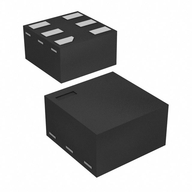
- Package: SOT-23
- Essence: CMOS Technology
- Packaging/Quantity: Tape and Reel, 3000 units per reel
Specifications
- Supply Voltage: 1.65V to 5.5V
- Input Voltage: 0V to VDD
- Output Voltage: 0V to VDD
- Propagation Delay: 2.5ns (typical)
- Operating Temperature Range: -40°C to +85°C
Detailed Pin Configuration
The NC7SV05FHX has a total of 5 pins:
- Pin 1: Input A
- Pin 2: GND (Ground)
- Pin 3: Output Y
- Pin 4: VDD (Supply Voltage)
- Pin 5: Input B
Functional Features
- Provides logic level inversion for digital signals
- Supports low voltage operation, making it suitable for battery-powered devices
- Offers high-speed performance with low propagation delay
- Compatible with a wide range of input and output voltage levels
- Utilizes CMOS technology for improved power efficiency
Advantages and Disadvantages
Advantages
- Low power consumption
- Wide operating voltage range
- Small package size allows for space-saving designs
- High-speed operation
- Easy integration into existing circuits
Disadvantages
- Limited output current capability
- Sensitivity to electrostatic discharge (ESD)
- Not suitable for high-power applications
Working Principles
The NC7SV05FHX is an inverter gate that operates based on complementary metal-oxide-semiconductor (CMOS) technology. It consists of a PMOS (p-channel metal-oxide-semiconductor) transistor and an NMOS (n-channel metal-oxide-semiconductor) transistor. When the input signal is low, the PMOS transistor conducts and pulls the output voltage high. Conversely, when the input signal is high, the NMOS transistor conducts and pulls the output voltage low.
Detailed Application Field Plans
The NC7SV05FHX can be used in various applications, including:
- Battery-powered devices: Due to its low voltage operation and low power consumption, it is suitable for portable electronics such as smartphones, tablets, and wearables.
- Communication systems: It can be utilized in signal processing circuits, data transmission, and interface modules.
- Industrial automation: The inverter gate can be integrated into control systems, motor drives, and sensor interfaces.
- Automotive electronics: It finds application in vehicle control units, infotainment systems, and lighting controls.
- Internet of Things (IoT): The IC can be employed in IoT devices, smart home automation, and environmental monitoring systems.
Detailed and Complete Alternative Models
- SN74LVC1G04DBVR: Single Inverter Gate, SOT-23 package, 1.65V to 5.5V supply voltage range.
- MC74VHC1G14DFT1G: Schmitt Trigger Inverter, SOT-23 package, 2V to 5.5V supply voltage range.
- TC7SZ04FU: Hex Inverter, SOT-353 package, 1.65V to 5.5V supply voltage range.
(Note: This list is not exhaustive and there are several other alternative models available in the market.)
In conclusion, the NC7SV05FHX is a CMOS-based inverter gate that offers low voltage operation, high-speed performance, and compatibility with a wide range of input and output voltage levels. It finds application in various fields such as battery-powered devices, communication systems, industrial automation, automotive electronics, and IoT. While it has advantages like low power consumption and small package size, it also has limitations such as limited output current capability and sensitivity to ESD. Alternative models like SN74LVC1G04DBVR, MC74VHC1G14DFT1G, and TC7SZ04FU provide similar functionality and can be considered as alternatives to the NC7SV05FHX.
Sebutkan 10 pertanyaan dan jawaban umum terkait penerapan NC7SV05FHX dalam solusi teknis
Sure! Here are 10 common questions and answers related to the application of NC7SV05FHX in technical solutions:
Question: What is NC7SV05FHX?
- Answer: NC7SV05FHX is a single-gate, non-inverting buffer with open-drain output, commonly used in digital logic circuits.Question: What is the voltage supply range for NC7SV05FHX?
- Answer: The voltage supply range for NC7SV05FHX is typically between 1.65V and 5.5V.Question: What is the maximum output current of NC7SV05FHX?
- Answer: The maximum output current of NC7SV05FHX is typically around 32mA.Question: Can NC7SV05FHX be used as a level shifter?
- Answer: Yes, NC7SV05FHX can be used as a level shifter to convert signals between different voltage levels.Question: What is the propagation delay of NC7SV05FHX?
- Answer: The propagation delay of NC7SV05FHX is typically around 2.5ns.Question: Is NC7SV05FHX suitable for high-speed applications?
- Answer: Yes, NC7SV05FHX is designed for high-speed operation and can be used in various high-frequency applications.Question: Can NC7SV05FHX drive capacitive loads?
- Answer: Yes, NC7SV05FHX can drive small capacitive loads without any additional buffering.Question: What is the operating temperature range for NC7SV05FHX?
- Answer: The operating temperature range for NC7SV05FHX is typically between -40°C and 85°C.Question: Can NC7SV05FHX be used in battery-powered applications?
- Answer: Yes, NC7SV05FHX is suitable for battery-powered applications due to its low power consumption.Question: Is NC7SV05FHX available in different package options?
- Answer: Yes, NC7SV05FHX is available in various package options, such as SOT-23 and SC70, to accommodate different design requirements.
Please note that the answers provided here are general and may vary depending on specific datasheet specifications and application requirements.