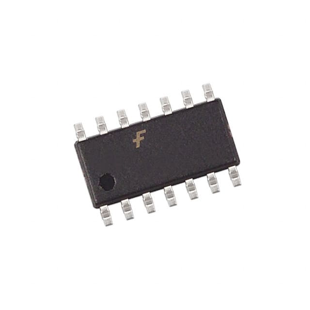
Lihat spesifikasi untuk detail produk.

MM74HC126SJX
Product Overview
- Category: Integrated Circuit
- Use: Logic Gate Buffer/Driver
- Characteristics: High-Speed, Quad 3-State Non-Inverting Buffer
- Package: SOIC (Small Outline Integrated Circuit)
- Essence: The MM74HC126SJX is a quad 3-state non-inverting buffer that operates at high speed and provides a convenient interface between different logic levels.
- Packaging/Quantity: The MM74HC126SJX is typically sold in reels of 2500 units.
Specifications
- Supply Voltage: 2V to 6V
- Input Voltage: 0V to Vcc
- Output Voltage: 0V to Vcc
- Operating Temperature Range: -40°C to +85°C
- Propagation Delay: 9ns (typical)
- Output Current: ±25mA
Pin Configuration
The MM74HC126SJX has a total of 14 pins, which are labeled as follows:
- 1A
- 1Y
- GND
- 2A
- 2Y
- 3A
- 3Y
- 4A
- 4Y
- GND
- 4OE
- 3OE
- Vcc
- 1OE
Functional Features
- Quad 3-state non-inverting buffer with separate output enable for each channel.
- High-speed operation makes it suitable for applications requiring fast signal transmission.
- Provides voltage level shifting capability, allowing interfacing between different logic families.
- 3-state outputs allow multiple devices to share a common bus without interference.
Advantages and Disadvantages
Advantages
- High-speed operation enables efficient signal transmission.
- 3-state outputs provide flexibility in bus sharing applications.
- Wide operating voltage range allows compatibility with various systems.
- Small package size (SOIC) makes it suitable for space-constrained designs.
Disadvantages
- Limited output current may not be sufficient for driving heavy loads.
- Lack of built-in protection features may require additional circuitry for robustness.
Working Principles
The MM74HC126SJX operates as a buffer, amplifying and reshaping input signals to match the desired logic levels. It uses CMOS technology, which provides high-speed operation and low power consumption. The separate output enable pins allow individual control of each channel, enabling 3-state functionality.
Detailed Application Field Plans
The MM74HC126SJX is commonly used in various digital systems and communication devices. Some specific application areas include:
- Microcontroller interfacing
- Data bus buffering
- Address decoding
- Signal level shifting
- Clock distribution
Detailed and Complete Alternative Models
- SN74HC126N: Similar quad 3-state non-inverting buffer from Texas Instruments.
- CD74HC126E: Quad 3-state non-inverting buffer from Texas Instruments.
- 74HCT126: Quad 3-state non-inverting buffer with TTL compatibility.
These alternative models offer similar functionality and can be used as substitutes for the MM74HC126SJX in various applications.
In conclusion, the MM74HC126SJX is a high-speed quad 3-state non-inverting buffer that provides voltage level shifting capability and flexible bus sharing. Its small package size and wide operating voltage range make it suitable for a variety of digital systems and communication devices. However, its limited output current and lack of built-in protection features should be considered when designing robust circuits.
Sebutkan 10 pertanyaan dan jawaban umum terkait penerapan MM74HC126SJX dalam solusi teknis
Sure! Here are 10 common questions and answers related to the application of MM74HC126SJX in technical solutions:
Q: What is MM74HC126SJX? A: MM74HC126SJX is a quad buffer/line driver IC (integrated circuit) that can be used for signal buffering and level shifting applications.
Q: What is the operating voltage range of MM74HC126SJX? A: The operating voltage range of MM74HC126SJX is typically between 2V and 6V.
Q: Can MM74HC126SJX handle both digital and analog signals? A: Yes, MM74HC126SJX can handle both digital and analog signals, making it versatile for various applications.
Q: How many buffer/line driver circuits are there in MM74HC126SJX? A: MM74HC126SJX consists of four independent buffer/line driver circuits.
Q: What is the maximum output current capability of MM74HC126SJX? A: The maximum output current capability of MM74HC126SJX is typically around 6mA.
Q: Can MM74HC126SJX be used for bidirectional communication? A: No, MM74HC126SJX is unidirectional and can only be used for one-way signal transmission.
Q: What is the typical propagation delay of MM74HC126SJX? A: The typical propagation delay of MM74HC126SJX is around 9ns.
Q: Is MM74HC126SJX compatible with TTL (Transistor-Transistor Logic) inputs? A: Yes, MM74HC126SJX is compatible with TTL inputs, making it suitable for interfacing with TTL logic circuits.
Q: Can MM74HC126SJX be used in high-speed applications? A: Yes, MM74HC126SJX is designed for high-speed operation and can be used in applications requiring fast signal switching.
Q: What is the package type of MM74HC126SJX? A: MM74HC126SJX is available in a 14-pin SOIC (Small Outline Integrated Circuit) package.
Please note that the answers provided here are general and may vary depending on specific datasheet specifications and application requirements.

