

Lihat spesifikasi untuk detail produk.
MC74HC1G04DTT1G
Product Overview
- Category: Integrated Circuit (IC)
- Use: Logic Gate
- Characteristics: High-Speed, CMOS Technology
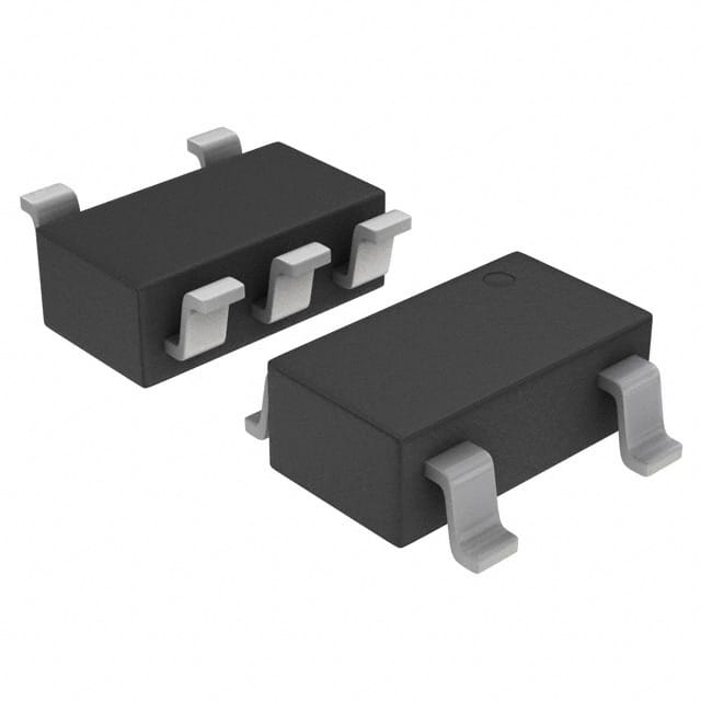
- Package: SOT-23-5
- Essence: Inverter Gate
- Packaging/Quantity: Tape and Reel, 3000 units per reel
Specifications
- Supply Voltage: 2.0V to 6.0V
- Input Voltage: 0V to VCC
- Output Voltage: 0V to VCC
- Operating Temperature Range: -55°C to +125°C
- Propagation Delay Time: 8 ns (typical)
- Quiescent Current: 1 µA (maximum)
Detailed Pin Configuration
The MC74HC1G04DTT1G has a total of 5 pins arranged as follows:
____
   1 |    |
   2 |    |
   3 |    |
   4 |    |
   5 |____|
Pin Description: 1. Input (A) 2. Ground (GND) 3. Output (Y) 4. Not Connected (NC) 5. Power Supply (VCC)
Functional Features
The MC74HC1G04DTT1G is a high-speed CMOS inverter gate. It provides logic inversion with fast switching speeds, making it suitable for various digital applications. The device operates within a wide voltage range and exhibits low power consumption.
Advantages and Disadvantages
Advantages: - High-speed operation - Low power consumption - Wide operating voltage range - Compact package size
Disadvantages: - Limited number of inputs/outputs - Not suitable for high-power applications
Working Principles
The MC74HC1G04DTT1G utilizes CMOS technology to achieve high-speed logic inversion. When the input voltage is low, the output voltage is high, and vice versa. The device operates by controlling the flow of current through its internal transistors, resulting in the desired logic inversion.
Detailed Application Field Plans
The MC74HC1G04DTT1G can be used in various digital applications, including but not limited to: - Logic level conversion - Clock signal generation - Signal buffering - Waveform shaping
Detailed and Complete Alternative Models
- SN74LVC1G04DBVR - Single Inverter Gate, SOT-23-5 package
- CD74HC1G04M96 - Single Inverter Gate, SOT-963 package
- TC7SZ04FU - Single Inverter Gate, SOT-353 package
- 74AUP1G04GW - Single Inverter Gate, SOT-753 package
These alternative models offer similar functionality and characteristics to the MC74HC1G04DTT1G, providing users with options based on their specific requirements.
In conclusion, the MC74HC1G04DTT1G is a high-speed CMOS inverter gate that offers logic inversion with fast switching speeds. It operates within a wide voltage range and consumes low power. With its compact package size, it finds applications in various digital circuits requiring logic level conversion, clock signal generation, signal buffering, and waveform shaping. Users also have alternative models available to suit their specific needs.
Sebutkan 10 pertanyaan dan jawaban umum terkait penerapan MC74HC1G04DTT1G dalam solusi teknis
Sure! Here are 10 common questions and answers related to the application of MC74HC1G04DTT1G in technical solutions:
Q1: What is MC74HC1G04DTT1G? A1: MC74HC1G04DTT1G is a logic gate IC (Integrated Circuit) that consists of six inverters. It is commonly used in digital electronics for signal inversion or buffering.
Q2: What is the operating voltage range of MC74HC1G04DTT1G? A2: The operating voltage range of MC74HC1G04DTT1G is typically between 2V and 6V.
Q3: What is the maximum output current of MC74HC1G04DTT1G? A3: The maximum output current of MC74HC1G04DTT1G is around 5.2mA.
Q4: Can MC74HC1G04DTT1G be used as a level shifter? A4: Yes, MC74HC1G04DTT1G can be used as a level shifter to convert signals from one voltage level to another.
Q5: What is the propagation delay of MC74HC1G04DTT1G? A5: The propagation delay of MC74HC1G04DTT1G is typically around 9ns.
Q6: Can MC74HC1G04DTT1G be used in high-speed applications? A6: Yes, MC74HC1G04DTT1G can be used in high-speed applications as it has a relatively fast switching speed.
Q7: Is MC74HC1G04DTT1G compatible with other logic families? A7: Yes, MC74HC1G04DTT1G is compatible with other logic families such as TTL (Transistor-Transistor Logic) and CMOS (Complementary Metal-Oxide-Semiconductor).
Q8: Can MC74HC1G04DTT1G drive capacitive loads? A8: Yes, MC74HC1G04DTT1G can drive small capacitive loads. However, for larger capacitive loads, additional buffering may be required.
Q9: What is the temperature range for operating MC74HC1G04DTT1G? A9: The temperature range for operating MC74HC1G04DTT1G is typically between -40°C and 85°C.
Q10: Can MC74HC1G04DTT1G be used in battery-powered applications? A10: Yes, MC74HC1G04DTT1G can be used in battery-powered applications as it operates at low power and has a wide supply voltage range.
Please note that these answers are general and may vary depending on specific datasheet specifications or application requirements.