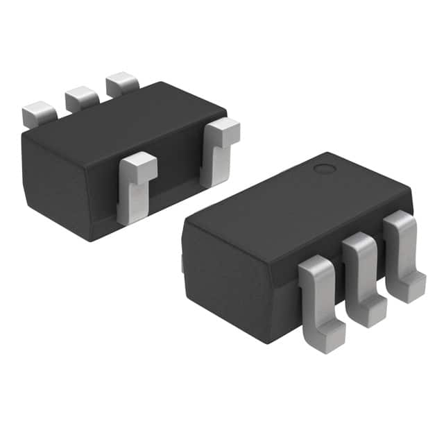
Lihat spesifikasi untuk detail produk.

MC74HC1G04DFT1G
Product Overview
- Category: Integrated Circuit (IC)
- Use: Logic Gate
- Characteristics: High-Speed, Low-Power, Inverter
- Package: SOT-353
- Essence: Single Gate Inverter
- Packaging/Quantity: Tape and Reel, 3000 pieces per reel
Specifications
- Supply Voltage Range: 2.0V to 6.0V
- Input Voltage Range: 0V to VCC
- Output Voltage Range: 0V to VCC
- Maximum Quiescent Current: 1µA at 5.5V
- Maximum Propagation Delay: 8ns at 4.5V
- Operating Temperature Range: -40°C to +85°C
Detailed Pin Configuration
The MC74HC1G04DFT1G has a total of 5 pins:
- GND (Ground): Connected to the ground reference voltage.
- A (Input): Input pin for the logic signal.
- Y (Output): Output pin for the inverted logic signal.
- NC (No Connection): This pin is not connected and should be left unconnected.
- VCC (Power Supply): Connected to the positive supply voltage.
Functional Features
The MC74HC1G04DFT1G is a high-speed CMOS inverter that operates with low power consumption. It provides a single gate inverter function, which means it takes an input logic signal and produces the inverted output logic signal. The device is designed to operate within a wide supply voltage range, making it suitable for various applications.
Advantages and Disadvantages
Advantages: - High-speed operation allows for quick signal processing. - Low-power consumption makes it energy-efficient. - Small package size saves board space. - Wide supply voltage range provides flexibility in different applications.
Disadvantages: - Limited functionality as it only performs the inverter function. - Not suitable for high-voltage applications due to its low voltage rating.
Working Principles
The MC74HC1G04DFT1G utilizes CMOS technology to achieve high-speed and low-power operation. It consists of a complementary pair of MOS transistors that form an inverter circuit. When the input logic signal is high, the output is low, and vice versa. The device operates by controlling the flow of current through these transistors based on the input voltage level.
Detailed Application Field Plans
The MC74HC1G04DFT1G can be used in various digital logic applications, including but not limited to: - Signal inversion in digital circuits. - Level shifting between different voltage domains. - Buffering and signal conditioning. - Clock signal generation and distribution. - Logic signal amplification.
Detailed and Complete Alternative Models
- SN74LVC1G04DBVR: Single Gate Inverter, SOT-23 package, 3000 pieces per reel.
- CD74HC1G04M96: Single Gate Inverter, SOT-963 package, 10000 pieces per reel.
- TC7SZ04FU: Single Gate Inverter, SOT-353 package, 5000 pieces per reel.
- 74AUP1G04GW: Single Gate Inverter, SOT-753 package, 2500 pieces per reel.
- HCF4049UBM1: Hex Inverting Buffer, SOIC-16 package, 2000 pieces per reel.
These alternative models provide similar functionality to the MC74HC1G04DFT1G and can be considered as replacements depending on specific requirements and availability.
In conclusion, the MC74HC1G04DFT1G is a high-speed, low-power CMOS inverter integrated circuit. It is widely used in digital logic applications for signal inversion and level shifting. With its small package size and wide supply voltage range, it offers flexibility and efficiency in various electronic designs.
Sebutkan 10 pertanyaan dan jawaban umum terkait penerapan MC74HC1G04DFT1G dalam solusi teknis
Sure! Here are 10 common questions and answers related to the application of MC74HC1G04DFT1G in technical solutions:
Q1: What is MC74HC1G04DFT1G? A1: MC74HC1G04DFT1G is a logic gate IC (Integrated Circuit) that consists of six inverters. It is commonly used in digital electronics for signal inversion and buffering.
Q2: What is the operating voltage range of MC74HC1G04DFT1G? A2: The operating voltage range of MC74HC1G04DFT1G is typically between 2V and 6V.
Q3: Can MC74HC1G04DFT1G be used as a level shifter? A3: Yes, MC74HC1G04DFT1G can be used as a level shifter to convert signals from one voltage level to another.
Q4: What is the maximum output current of MC74HC1G04DFT1G? A4: The maximum output current of MC74HC1G04DFT1G is around 5mA.
Q5: Can MC74HC1G04DFT1G be used in high-speed applications? A5: Yes, MC74HC1G04DFT1G is suitable for high-speed applications due to its fast propagation delay and transition times.
Q6: Is MC74HC1G04DFT1G compatible with TTL logic levels? A6: Yes, MC74HC1G04DFT1G is compatible with TTL (Transistor-Transistor Logic) logic levels, making it versatile for interfacing with different types of devices.
Q7: Can MC74HC1G04DFT1G be used in battery-powered applications? A7: Yes, MC74HC1G04DFT1G is commonly used in battery-powered applications due to its low power consumption.
Q8: What is the package type of MC74HC1G04DFT1G? A8: MC74HC1G04DFT1G is available in a small SOT-353 package, which is suitable for space-constrained designs.
Q9: Can MC74HC1G04DFT1G be used in temperature-sensitive environments? A9: Yes, MC74HC1G04DFT1G has a wide operating temperature range of -40°C to 125°C, making it suitable for various temperature-sensitive applications.
Q10: Are there any recommended decoupling capacitors for MC74HC1G04DFT1G? A10: It is generally recommended to use a 0.1μF ceramic capacitor placed close to the VCC and GND pins of MC74HC1G04DFT1G to ensure stable operation and reduce noise.
Please note that these answers are general and may vary depending on specific application requirements.

