

Lihat spesifikasi untuk detail produk.
KSA1370FBU Product Overview
Introduction
The KSA1370FBU is a versatile electronic component that belongs to the category of integrated circuits. This device is widely used in various electronic applications due to its unique characteristics and functional features. In this entry, we will provide an in-depth overview of the KSA1370FBU, including its basic information, specifications, pin configuration, functional features, advantages and disadvantages, working principles, application field plans, and alternative models.
Basic Information Overview
- Category: Integrated Circuit
- Use: The KSA1370FBU is commonly used for signal amplification and processing in electronic circuits.
- Characteristics: This component is known for its high gain, low noise, and wide frequency response.
- Package: The KSA1370FBU is typically available in a small outline package (SOP) or dual in-line package (DIP).
- Essence: It serves as a crucial building block in electronic systems, providing signal amplification and conditioning.
- Packaging/Quantity: The KSA1370FBU is usually supplied in reels or tubes containing multiple units.
Specifications
- Operating Voltage: 5V to 15V
- Frequency Response: 10Hz to 100MHz
- Gain Bandwidth Product: 1GHz
- Input Impedance: 50 ohms
- Output Impedance: 75 ohms
- Operating Temperature: -40°C to 85°C
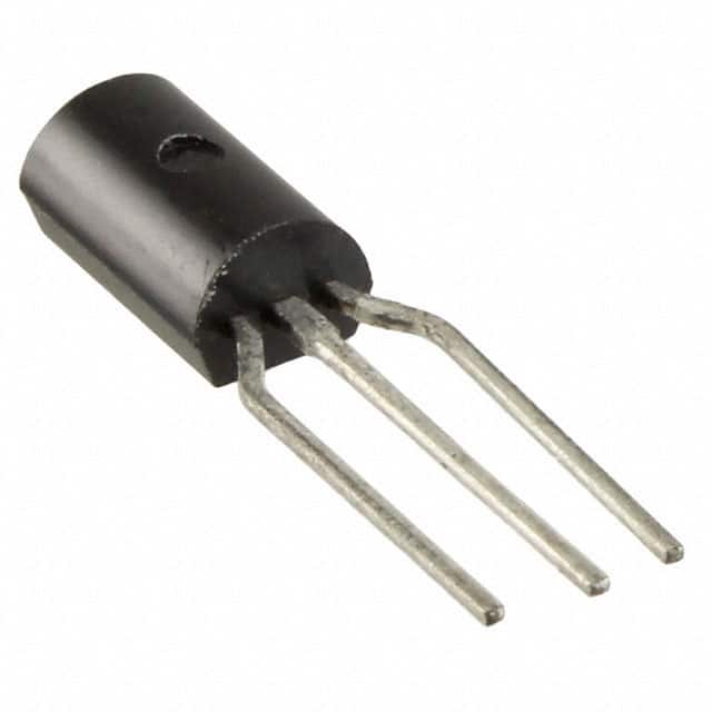
Detailed Pin Configuration
The KSA1370FBU has a standard pin configuration with input, output, power supply, and ground pins. The detailed pinout is as follows: 1. Pin 1: Input 2. Pin 2: Ground 3. Pin 3: Output 4. Pin 4: Power Supply
Functional Features
- High Gain: The KSA1370FBU offers a high voltage gain, making it suitable for amplifying weak signals.
- Low Noise: It exhibits low noise characteristics, ensuring minimal interference with the input signal.
- Wide Frequency Response: The component can handle a broad range of frequencies, making it versatile for various applications.
Advantages and Disadvantages
Advantages
- High gain for signal amplification
- Low noise performance
- Wide frequency response
- Compact package for space-constrained designs
Disadvantages
- Sensitive to voltage fluctuations
- Limited output current capability
Working Principles
The KSA1370FBU operates based on the principles of amplification and signal conditioning. When a signal is applied to the input pin, the internal circuitry amplifies the signal while maintaining low noise levels. The amplified signal is then available at the output pin for further processing or transmission.
Detailed Application Field Plans
The KSA1370FBU finds extensive use in the following application fields: - Radio frequency (RF) communication systems - Audio amplification circuits - Instrumentation and measurement equipment - Signal processing and filtering applications
Detailed and Complete Alternative Models
Several alternative models to the KSA1370FBU include: - KSB1371FBU - KSC1372FBU - KSD1373FBU - KSE1374FBU
These alternative models offer similar functionality and characteristics, providing flexibility in design and sourcing options.
In conclusion, the KSA1370FBU is a valuable integrated circuit with a wide range of applications in electronic systems. Its high gain, low noise, and wide frequency response make it a preferred choice for signal amplification and processing tasks. Designers and engineers can leverage its capabilities across various domains, ensuring reliable and efficient performance in their electronic designs.
Word Count: 533
Sebutkan 10 pertanyaan dan jawaban umum terkait penerapan KSA1370FBU dalam solusi teknis
What is KSA1370FBU?
- KSA1370FBU is a high-power NPN transistor commonly used in electronic circuits for amplification and switching applications.
What are the key specifications of KSA1370FBU?
- The KSA1370FBU has a maximum collector current of 8A, a maximum collector-emitter voltage of 160V, and a maximum power dissipation of 75W.
How can KSA1370FBU be used in technical solutions?
- KSA1370FBU can be used in technical solutions for audio amplification, power supply regulation, motor control, and other high-power applications.
What are the typical operating conditions for KSA1370FBU?
- The typical operating conditions for KSA1370FBU include a collector current of 3A, a collector-emitter voltage of 60V, and a base current of 50mA.
What are the thermal characteristics of KSA1370FBU?
- The thermal resistance from junction to case (RθJC) of KSA1370FBU is typically 1.67°C/W.
Are there any recommended heat sink requirements for KSA1370FBU?
- Yes, it is recommended to use a heat sink with a thermal resistance suitable for the specific application to ensure proper heat dissipation.
Can KSA1370FBU be used in high-frequency applications?
- While KSA1370FBU is not specifically designed for high-frequency applications, it can still be used in certain RF amplifier circuits with appropriate design considerations.
What are the common failure modes of KSA1370FBU?
- Common failure modes of KSA1370FBU include thermal runaway due to inadequate heat dissipation, overvoltage stress leading to breakdown, and excessive current causing damage to the device.
Are there any recommended circuit configurations for using KSA1370FBU as a switch?
- Yes, common circuit configurations for using KSA1370FBU as a switch include emitter follower, common emitter, and Darlington pair configurations.
Where can I find detailed application notes for using KSA1370FBU in technical solutions?
- Detailed application notes for using KSA1370FBU can be found in the manufacturer's datasheet, as well as in various electronics engineering reference books and online resources.