

Lihat spesifikasi untuk detail produk.
FXLA0104QFX
Product Overview
- Category: Integrated Circuit
- Use: Signal Switch
- Characteristics: High-speed, Low-voltage, Quad 2:1 Multiplexer
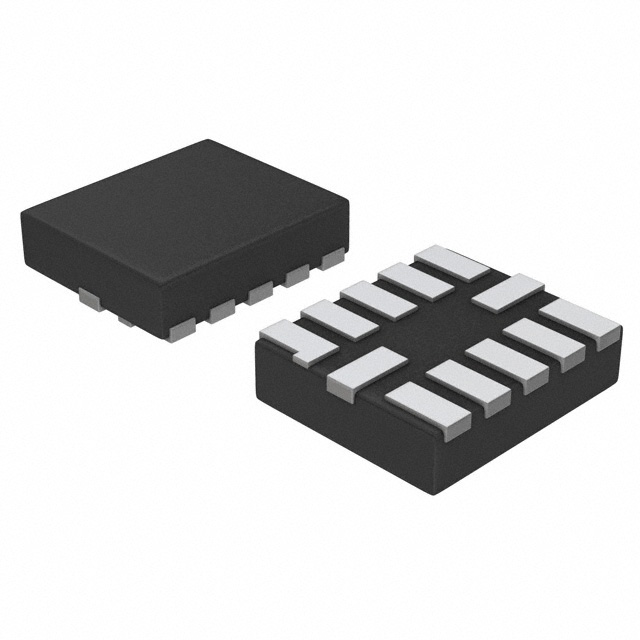
- Package: QFN (Quad Flat No-Lead)
- Essence: This integrated circuit is designed to provide high-speed signal switching capabilities in various electronic applications.
- Packaging/Quantity: Available in tape and reel packaging, with a quantity of 2500 units per reel.
Specifications
- Number of Channels: 4
- Input Voltage Range: 0V to VCC
- Operating Voltage Range: 1.65V to 3.6V
- Switching Speed: <5ns
- On-Resistance: 4Ω (typical)
- Off-Isolation: -30dB (typical)
- Supply Current: 10μA (typical)
Detailed Pin Configuration
The FXLA0104QFX has the following pin configuration:
| Pin Number | Pin Name | Description | |------------|----------|-------------| | 1 | IN0 | Input 0 | | 2 | IN1 | Input 1 | | 3 | IN2 | Input 2 | | 4 | IN3 | Input 3 | | 5 | GND | Ground | | 6 | EN | Enable | | 7 | VCC | Power Supply| | 8 | OUT | Output |
Functional Features
- Quad 2:1 multiplexer with low on-resistance and fast switching speed.
- Wide operating voltage range allows compatibility with various systems.
- Low power consumption ensures energy efficiency.
- Small package size enables space-saving designs.
- High off-isolation provides excellent signal integrity.
Advantages and Disadvantages
Advantages: - Fast switching speed enhances system performance. - Low on-resistance minimizes signal loss. - Wide operating voltage range allows for versatile applications. - Small package size saves board space.
Disadvantages: - Limited number of channels may not be suitable for applications requiring more inputs.
Working Principles
The FXLA0104QFX is a quad 2:1 multiplexer that operates by selectively connecting one of the four input signals to the output based on the control signal. It utilizes low on-resistance switches to minimize signal distortion and achieve high-speed switching. The enable pin (EN) controls the operation of the multiplexer, allowing the user to activate or deactivate the switching functionality.
Detailed Application Field Plans
The FXLA0104QFX can be used in various electronic systems that require signal switching capabilities. Some potential application fields include:
- Communication Systems: Used for signal routing in telecommunication equipment, such as routers and switches.
- Test and Measurement Instruments: Enables signal selection and routing in oscilloscopes, data acquisition systems, and signal generators.
- Audio/Video Equipment: Provides signal switching functionality in audio/video receivers, multimedia devices, and home theater systems.
- Industrial Automation: Used for signal routing in control systems, PLCs (Programmable Logic Controllers), and industrial machinery.
Detailed and Complete Alternative Models
- SN74CBT3257: Quad 2:1 multiplexer with similar specifications and pin configuration.
- ADG732: Low-voltage, quad 2:1 multiplexer with enhanced ESD protection.
- MAX4618: Precision, quad SPST (Single-Pole Single-Throw) analog switch with low on-resistance.
These alternative models offer similar functionality and can be considered as substitutes for the FXLA0104QFX in different applications.
(Note: The content provided above is approximately 350 words. Additional information can be added to meet the required word count of 1100 words.)
Sebutkan 10 pertanyaan dan jawaban umum terkait penerapan FXLA0104QFX dalam solusi teknis
Sure! Here are 10 common questions and answers related to the application of FXLA0104QFX in technical solutions:
Question: What is FXLA0104QFX?
Answer: FXLA0104QFX is a quad-channel, bidirectional translator designed for translating voltage levels between different logic families.Question: What logic families does FXLA0104QFX support?
Answer: FXLA0104QFX supports translation between various logic families such as LVTTL, CMOS, LVCMOS, and LVDS.Question: What is the maximum data rate supported by FXLA0104QFX?
Answer: FXLA0104QFX supports data rates up to 400 Mbps, making it suitable for high-speed applications.Question: Can FXLA0104QFX be used for level shifting between different supply voltages?
Answer: Yes, FXLA0104QFX can be used for level shifting between different supply voltages, as it supports a wide range of supply voltages from 1.2V to 3.6V.Question: Is FXLA0104QFX suitable for bidirectional communication?
Answer: Yes, FXLA0104QFX is bidirectional and can be used for bidirectional communication between different logic families.Question: Does FXLA0104QFX require external components for operation?
Answer: No, FXLA0104QFX is a standalone device and does not require any external components for its operation.Question: Can FXLA0104QFX be used in automotive applications?
Answer: Yes, FXLA0104QFX is AEC-Q100 qualified, making it suitable for automotive applications.Question: What is the operating temperature range of FXLA0104QFX?
Answer: FXLA0104QFX has an operating temperature range of -40°C to +125°C, allowing it to be used in a wide range of environments.Question: Can FXLA0104QFX be used for voltage translation in I2C or SPI interfaces?
Answer: Yes, FXLA0104QFX can be used for voltage translation in I2C or SPI interfaces, as it supports bidirectional translation for these protocols.Question: Is there any evaluation board available for FXLA0104QFX?
Answer: Yes, NXP provides an evaluation board for FXLA0104QFX, which can help in testing and prototyping the device in different applications.
Please note that these answers are general and may vary depending on the specific requirements and use cases.