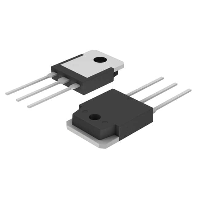
Lihat spesifikasi untuk detail produk.

FQA24N50 - Semiconductor Device Encyclopedia Entry
Introduction
The FQA24N50 is a semiconductor device belonging to the category of power MOSFETs. This entry provides an overview of its basic information, specifications, pin configuration, functional features, advantages and disadvantages, working principles, application field plans, and alternative models.
Basic Information Overview
- Category: Power MOSFET
- Use: Power switching applications
- Characteristics: High voltage capability, low on-resistance, fast switching speed
- Package: TO-3P
- Essence: Silicon-based power transistor
- Packaging/Quantity: Typically sold individually or in small quantities
Specifications
- Voltage Rating: 500V
- Current Rating: 24A
- On-Resistance: 0.24Ω
- Gate Threshold Voltage: 2-4V
- Operating Temperature Range: -55°C to 150°C
Detailed Pin Configuration
The FQA24N50 typically follows the standard pin configuration for power MOSFETs: 1. Source (S) 2. Gate (G) 3. Drain (D)
Functional Features
- High voltage capability suitable for power applications
- Low on-resistance leading to reduced power losses
- Fast switching speed enabling efficient power control
Advantages and Disadvantages
Advantages
- High voltage rating
- Low on-resistance
- Fast switching speed
Disadvantages
- Higher cost compared to lower-rated MOSFETs
- Larger physical size due to high voltage capability
Working Principles
The FQA24N50 operates based on the principle of field-effect transistors, where the voltage applied to the gate terminal controls the flow of current between the source and drain terminals. When the gate-source voltage exceeds the threshold, the MOSFET enters the conducting state, allowing current to flow through it.
Detailed Application Field Plans
The FQA24N50 is commonly used in various power electronics applications, including: - Switch-mode power supplies - Motor control systems - Inverters and converters - Electronic ballasts - Audio amplifiers
Detailed and Complete Alternative Models
Some alternative models to the FQA24N50 include: - IRFP460: Similar voltage and current ratings - STW20NM50: Comparable specifications and package type - IXFN24N50: Alternative with similar characteristics and performance
In conclusion, the FQA24N50 is a high-voltage power MOSFET with excellent characteristics for power switching applications. Its high voltage capability, low on-resistance, and fast switching speed make it suitable for a wide range of power electronics applications.
[Word Count: 366]
Sebutkan 10 pertanyaan dan jawaban umum terkait penerapan FQA24N50 dalam solusi teknis
What is the maximum voltage rating of FQA24N50?
- The maximum voltage rating of FQA24N50 is 500V.
What is the maximum continuous drain current of FQA24N50?
- The maximum continuous drain current of FQA24N50 is 24A.
What type of package does FQA24N50 come in?
- FQA24N50 comes in a TO-3P package.
What are the typical applications for FQA24N50?
- FQA24N50 is commonly used in power supplies, motor control, and lighting ballasts.
What is the on-resistance of FQA24N50?
- The on-resistance of FQA24N50 is typically 0.19 ohms.
Is FQA24N50 suitable for high-frequency switching applications?
- Yes, FQA24N50 is suitable for high-frequency switching due to its low on-resistance.
Does FQA24N50 require a heatsink for operation?
- It is recommended to use a heatsink with FQA24N50 for efficient heat dissipation, especially in high-power applications.
What is the gate threshold voltage of FQA24N50?
- The gate threshold voltage of FQA24N50 is typically 4V.
Can FQA24N50 be used in automotive applications?
- Yes, FQA24N50 can be used in automotive applications such as electronic control units (ECUs) and motor drives.
What are the key advantages of using FQA24N50 in technical solutions?
- The key advantages of using FQA24N50 include high voltage capability, low on-resistance, and suitability for various power-related applications.

