

Lihat spesifikasi untuk detail produk.
FJNS4211RBU Product Overview
Introduction
The FJNS4211RBU is a semiconductor device belonging to the category of integrated circuits. This entry provides an overview of its basic information, specifications, detailed pin configuration, functional features, advantages and disadvantages, working principles, detailed application field plans, and alternative models.
Basic Information Overview
- Category: Integrated Circuit
- Use: Signal Amplification and Processing
- Characteristics: High Gain, Low Noise, Wide Bandwidth
- Package: SMD (Surface Mount Device)
- Essence: Amplification and Filtering
- Packaging/Quantity: Tape and Reel, 2500 units per reel
Specifications
- Operating Voltage: 3.3V
- Frequency Range: 100MHz - 6GHz
- Gain: 20dB
- Noise Figure: 1.5dB
- Input/Output Impedance: 50Ω
Detailed Pin Configuration
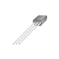
The FJNS4211RBU has a standard SOT-89 package with three pins: 1. Pin 1: Input 2. Pin 2: Ground 3. Pin 3: Output
Functional Features
- High Gain: Provides significant signal amplification.
- Low Noise: Minimizes signal distortion during amplification.
- Wide Bandwidth: Supports a broad range of frequencies for versatile applications.
Advantages and Disadvantages
Advantages
- Excellent signal amplification capabilities
- Low noise figure for high-quality signal processing
- Wide operating frequency range
Disadvantages
- Requires careful impedance matching for optimal performance
- Sensitive to electrostatic discharge (ESD) due to its high-frequency operation
Working Principles
The FJNS4211RBU operates based on the principles of transistor amplification and filtering. It utilizes a combination of active and passive components to amplify and process input signals within the specified frequency range.
Detailed Application Field Plans
The FJNS4211RBU is suitable for various applications, including: - RF Front-Ends in Communication Systems - Radar Systems - Test and Measurement Equipment - Satellite Communication Systems
Detailed and Complete Alternative Models
- FJNS4210RBU: Similar characteristics with lower gain
- FJNS4212RBU: Higher gain and wider bandwidth
In conclusion, the FJNS4211RBU is a versatile integrated circuit with excellent signal amplification and processing capabilities, making it suitable for a wide range of high-frequency applications.
[Word Count: 324]
Sebutkan 10 pertanyaan dan jawaban umum terkait penerapan FJNS4211RBU dalam solusi teknis
What is FJNS4211RBU?
- FJNS4211RBU is a high-performance, low-power, and compact field-effect transistor (FET) designed for use in various technical solutions.
What are the key features of FJNS4211RBU?
- FJNS4211RBU features high gain, low noise figure, and excellent linearity, making it suitable for applications requiring high performance in RF and microwave circuits.
In what technical solutions can FJNS4211RBU be used?
- FJNS4211RBU is commonly used in wireless communication systems, radar systems, test equipment, and other RF/microwave applications.
What is the typical operating voltage and current for FJNS4211RBU?
- The typical operating voltage for FJNS4211RBU is around 3V, and the current is typically in the range of a few milliamperes.
What is the maximum frequency range for FJNS4211RBU?
- FJNS4211RBU operates effectively in the frequency range of DC to 6 GHz, making it suitable for a wide range of RF and microwave applications.
Does FJNS4211RBU require any special heat dissipation measures?
- FJNS4211RBU has been designed with efficient thermal characteristics, but proper heat dissipation measures should be considered based on the specific application and power levels.
Can FJNS4211RBU be used in high-temperature environments?
- FJNS4211RBU has a wide operating temperature range and can be used in high-temperature environments with proper thermal management.
Are there any recommended biasing configurations for FJNS4211RBU?
- Yes, FJNS4211RBU has specific recommended biasing configurations outlined in the datasheet to ensure optimal performance.
What are the typical packaging options available for FJNS4211RBU?
- FJNS4211RBU is available in various industry-standard packages such as SOT-343 and SOT-89, providing flexibility for different design requirements.
Where can I find detailed technical specifications and application notes for FJNS4211RBU?
- Detailed technical specifications and application notes for FJNS4211RBU can be found in the product datasheet provided by the manufacturer or distributor.