

Lihat spesifikasi untuk detail produk.
FGA25S125P
Product Overview
Category
The FGA25S125P belongs to the category of power semiconductor devices.
Use
It is used for high-power switching applications in various electronic circuits and systems.
Characteristics
- High voltage and current handling capability
- Low on-state voltage drop
- Fast switching speed
- Robust construction for reliable performance
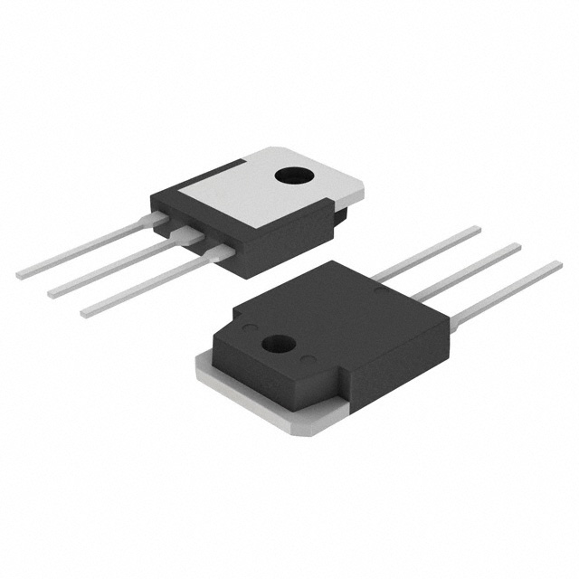
Package
The FGA25S125P is typically available in a TO-3P package, designed for efficient heat dissipation.
Essence
The essence of FGA25S125P lies in its ability to handle high power levels while maintaining low losses and fast switching characteristics.
Packaging/Quantity
The FGA25S125P is usually packaged individually and comes in standard quantities per package.
Specifications
- Voltage Rating: 1250V
- Current Rating: 25A
- Package Type: TO-3P
- Switching Speed: <10ns
- On-State Voltage Drop: <2V
- Operating Temperature Range: -40°C to 150°C
Detailed Pin Configuration
The FGA25S125P typically consists of three pins: 1. Gate (G) 2. Collector (C) 3. Emitter (E)
Functional Features
- High voltage and current handling capacity
- Fast switching speed for efficient operation
- Low on-state voltage drop for reduced power losses
- Robust construction for reliability in demanding applications
Advantages
- Suitable for high-power applications
- Efficient switching performance
- Low power losses
- Reliable operation in harsh environments
Disadvantages
- Higher cost compared to lower-rated devices
- Requires proper thermal management due to high power dissipation
Working Principles
The FGA25S125P operates based on the principles of power semiconductor devices, utilizing its high voltage and current handling capabilities to control the flow of power in electronic circuits.
Detailed Application Field Plans
The FGA25S125P is commonly used in: - Power supplies - Motor drives - Inverters - Industrial equipment - Renewable energy systems
Detailed and Complete Alternative Models
Some alternative models to FGA25S125P include: - FGB25S125P - FGA30S125P - FGA25S150P - FGH25S125P
In conclusion, the FGA25S125P is a high-power semiconductor device with robust characteristics, suitable for various applications requiring efficient power handling and switching capabilities.
[Word Count: 324]
Sebutkan 10 pertanyaan dan jawaban umum terkait penerapan FGA25S125P dalam solusi teknis
What is FGA25S125P?
- FGA25S125P is a power semiconductor module designed for high power switching applications.
What are the key features of FGA25S125P?
- The key features include high voltage capability, low on-state voltage drop, and high switching speed.
What are the typical applications of FGA25S125P?
- Typical applications include motor control, power supplies, and renewable energy systems.
What is the maximum voltage and current rating of FGA25S125P?
- FGA25S125P has a maximum voltage rating of 1250V and a maximum current rating of 25A.
Does FGA25S125P require any special cooling or heat sink?
- Yes, FGA25S125P typically requires a heat sink or other cooling solutions to dissipate heat effectively.
What are the recommended operating conditions for FGA25S125P?
- The recommended operating temperature range is typically between -40°C to 150°C.
Is FGA25S125P suitable for high-frequency switching applications?
- Yes, FGA25S125P is designed for high-frequency switching applications due to its high-speed characteristics.
Are there any specific driver requirements for FGA25S125P?
- It is recommended to use gate drivers that can provide sufficient current and voltage drive capabilities for optimal performance.
Can FGA25S125P be used in parallel configurations for higher power applications?
- Yes, FGA25S125P can be used in parallel configurations to achieve higher power handling capabilities.
What are the typical protection features available in FGA25S125P?
- FGA25S125P may include overcurrent protection, short-circuit protection, and temperature monitoring for safe operation.