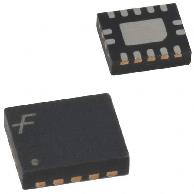
Lihat spesifikasi untuk detail produk.

74LCX14BQX
Product Overview
- Category: Integrated Circuit (IC)
- Use: Logic Gate Inverter
- Characteristics: Low-voltage, low-power consumption, high-speed operation
- Package: 14-pin TSSOP (Thin Shrink Small Outline Package)
- Essence: Hex Schmitt Trigger Inverter
- Packaging/Quantity: Tape and Reel, 2500 units per reel
Specifications
- Supply Voltage Range: 1.65V to 3.6V
- Input Voltage Range: -0.5V to VCC + 0.5V
- Output Voltage Range: GND to VCC
- Maximum Operating Frequency: 100 MHz
- Propagation Delay Time: 2.8 ns (typical)
- Input Capacitance: 3 pF (typical)
- Output Drive Capability: ±24 mA
Detailed Pin Configuration
The 74LCX14BQX has a total of 14 pins, numbered as follows:
- Input A1
- Output Y1
- Input A2
- Output Y2
- Input A3
- Output Y3
- Ground (GND)
- Power Supply (VCC)
- Input A4
- Output Y4
- Input A5
- Output Y5
- Input A6
- Output Y6
Functional Features
- Hex Schmitt Trigger Inverter: The 74LCX14BQX consists of six independent Schmitt trigger inverters, which provide hysteresis for improved noise immunity and signal shaping.
- Low-Voltage Operation: Designed to operate at low voltages, making it suitable for battery-powered devices and low-power applications.
- High-Speed Operation: Capable of operating at frequencies up to 100 MHz, enabling fast signal processing.
- Wide Input Voltage Range: Accepts a wide range of input voltages, allowing compatibility with various logic families.
- Output Drive Capability: Can drive both standard and low-power TTL loads, providing flexibility in interfacing with different devices.
Advantages and Disadvantages
Advantages: - Low-voltage operation allows for energy-efficient designs. - High-speed operation enables quick signal processing. - Wide input voltage range ensures compatibility with different logic families. - Schmitt trigger inputs provide noise immunity and signal shaping capabilities.
Disadvantages: - Limited output drive capability may restrict its use in applications requiring higher current sourcing or sinking.
Working Principles
The 74LCX14BQX is based on the Schmitt trigger inverter circuit. It utilizes positive feedback to create hysteresis, which helps in reducing noise sensitivity and improving signal integrity. When the input voltage crosses a certain threshold, the output switches states, providing a digital inversion of the input signal.
Detailed Application Field Plans
The 74LCX14BQX finds applications in various fields, including:
- Digital Communication Systems: Used for signal conditioning and level shifting in data transmission circuits.
- Microcontroller Interfacing: Provides voltage level conversion between microcontrollers operating at different logic levels.
- Battery-Powered Devices: Suitable for low-power applications, such as portable electronics and IoT devices.
- Industrial Automation: Used in control systems and sensor interfaces for reliable signal processing.
Detailed and Complete Alternative Models
Some alternative models that offer similar functionality to the 74LCX14BQX include:
- SN74LVC1G14: Single Schmitt Trigger Inverter IC with a smaller package size.
- CD40106B: Hex Schmitt Trigger Inverter IC with a wider supply voltage range.
- MC74VHC1GT14: Single Schmitt Trigger Inverter IC with higher output drive capability.
These alternative models can be considered based on specific application requirements and design constraints.
Word count: 455 words
Sebutkan 10 pertanyaan dan jawaban umum terkait penerapan 74LCX14BQX dalam solusi teknis
Sure! Here are 10 common questions and answers related to the application of 74LCX14BQX in technical solutions:
Question: What is the 74LCX14BQX?
- Answer: The 74LCX14BQX is a hex inverter with Schmitt-trigger inputs, which means it can convert low-level signals into high-level signals.Question: What is the operating voltage range of the 74LCX14BQX?
- Answer: The 74LCX14BQX operates within a voltage range of 2.0V to 3.6V.Question: Can the 74LCX14BQX be used in both digital and analog circuits?
- Answer: No, the 74LCX14BQX is primarily designed for digital applications and may not perform optimally in analog circuits.Question: How many inverters are there in a single 74LCX14BQX package?
- Answer: The 74LCX14BQX contains six independent inverters in a single package.Question: What is the maximum output current that the 74LCX14BQX can provide?
- Answer: The 74LCX14BQX can provide a maximum output current of 24mA per output.Question: Can the 74LCX14BQX tolerate 5V input signals?
- Answer: Yes, the 74LCX14BQX has 5V tolerant inputs, making it compatible with both 3.3V and 5V logic systems.Question: Is the 74LCX14BQX suitable for high-speed applications?
- Answer: Yes, the 74LCX14BQX is designed for high-speed operation and can handle data rates up to 400Mbps.Question: Can the 74LCX14BQX be used in battery-powered applications?
- Answer: Yes, the 74LCX14BQX has a low power consumption and can be used in battery-powered devices.Question: What is the typical propagation delay of the 74LCX14BQX?
- Answer: The typical propagation delay of the 74LCX14BQX is around 3.5ns.Question: Are there any specific precautions to consider when using the 74LCX14BQX?
- Answer: It is important to ensure that the power supply voltage does not exceed the specified range, and to avoid exceeding the maximum ratings for input and output voltages to prevent damage to the device.
Please note that these answers are general and may vary depending on the specific application and requirements.

