

Lihat spesifikasi untuk detail produk.
Encyclopedia Entry: 74ABT2541CMTC
Product Information Overview
- Category: Integrated Circuit (IC)
- Use: Logic Level Translator
- Characteristics: High-speed, low-power consumption
- Package: CMTC (Ceramic Metric Thin Chip)
- Essence: Translates logic levels between different voltage domains
- Packaging/Quantity: Available in reels of 2500 units
Specifications
- Logic Family: ABT
- Number of Channels: 8
- Input Voltage Range (VIL): 0 - 2.4V
- Output Voltage Range (VOL): 0 - 3.6V
- Supply Voltage (VCC): 4.5 - 5.5V
- Operating Temperature Range: -40°C to +85°C
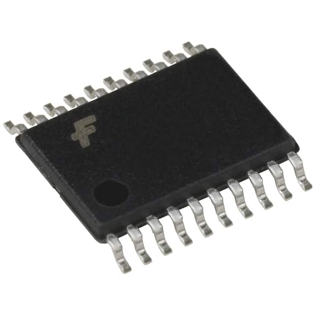
Detailed Pin Configuration
The 74ABT2541CMTC has a total of 20 pins, which are assigned as follows:
- Pin 1: Output Y0
- Pin 2: Output Y1
- Pin 3: Output Y2
- Pin 4: Output Y3
- Pin 5: Output Y4
- Pin 6: Output Y5
- Pin 7: Output Y6
- Pin 8: Output Y7
- Pin 9: GND (Ground)
- Pin 10: VCC (Supply Voltage)
- Pin 11: Input A0
- Pin 12: Input A1
- Pin 13: Input A2
- Pin 14: Input A3
- Pin 15: Input A4
- Pin 16: Input A5
- Pin 17: Input A6
- Pin 18: Input A7
- Pin 19: OE (Output Enable)
- Pin 20: GND (Ground)
Functional Features
The 74ABT2541CMTC is designed to translate logic levels between different voltage domains. It provides bidirectional level shifting, allowing seamless communication between devices operating at different voltage levels. The device features eight channels, each capable of translating a single signal.
Advantages and Disadvantages
Advantages: - High-speed operation enables efficient data transfer. - Low-power consumption makes it suitable for battery-powered applications. - Wide input and output voltage ranges provide flexibility in interfacing with various devices. - Compact CMTC package allows for space-saving integration.
Disadvantages: - Limited number of channels may not be sufficient for complex systems requiring multiple translations. - Requires careful consideration of voltage compatibility to avoid damage to connected devices.
Working Principles
The 74ABT2541CMTC utilizes a combination of MOSFETs and CMOS technology to achieve logic level translation. When an input signal is received, the device detects the voltage level and translates it to the corresponding voltage level on the output side. The direction of translation is determined by the state of the Output Enable (OE) pin.
Detailed Application Field Plans
The 74ABT2541CMTC finds application in various scenarios where logic level translation is required. Some potential fields of application include:
- Microcontroller Interfacing: Facilitating communication between microcontrollers operating at different voltage levels.
- Sensor Networks: Enabling connectivity between sensors and control units with varying voltage requirements.
- Industrial Automation: Integrating devices with different logic voltage standards in industrial control systems.
- IoT Devices: Bridging the gap between IoT devices operating at different voltage domains.
- Consumer Electronics: Supporting compatibility between devices with varying logic voltage levels.
Detailed and Complete Alternative Models
- 74LVC245: A similar logic level translator with 8 channels, compatible with a wider supply voltage range.
- SN74LV1T34: Single-channel level shifter suitable for low-power applications.
- CD4504B: Hex non-inverting level shifter with additional buffering capabilities.
These alternative models offer similar functionality to the 74ABT2541CMTC and can be considered based on specific application requirements.
Word Count: 411 words
Sebutkan 10 pertanyaan dan jawaban umum terkait penerapan 74ABT2541CMTC dalam solusi teknis
Sure! Here are 10 common questions and answers related to the application of 74ABT2541CMTC in technical solutions:
Q1: What is the purpose of the 74ABT2541CMTC integrated circuit? A1: The 74ABT2541CMTC is a octal buffer/line driver with 3-state outputs, designed for use as a bus interface or memory driver.
Q2: What is the maximum operating voltage for the 74ABT2541CMTC? A2: The maximum operating voltage for the 74ABT2541CMTC is 5.5 volts.
Q3: How many inputs and outputs does the 74ABT2541CMTC have? A3: The 74ABT2541CMTC has 8 inputs and 8 outputs.
Q4: Can the outputs of the 74ABT2541CMTC be disabled? A4: Yes, the outputs of the 74ABT2541CMTC can be disabled using the 3-state control input.
Q5: What is the output current capability of the 74ABT2541CMTC? A5: The 74ABT2541CMTC has a typical output current capability of ±24 mA.
Q6: Is the 74ABT2541CMTC compatible with TTL logic levels? A6: Yes, the 74ABT2541CMTC is compatible with both TTL and CMOS logic levels.
Q7: Can the 74ABT2541CMTC be used in high-speed applications? A7: Yes, the 74ABT2541CMTC is designed for high-speed operation and has a propagation delay of typically 3.5 ns.
Q8: Does the 74ABT2541CMTC have built-in protection against electrostatic discharge (ESD)? A8: Yes, the 74ABT2541CMTC has built-in ESD protection on all inputs and outputs.
Q9: Can the 74ABT2541CMTC be used in both parallel and serial data transfer applications? A9: Yes, the 74ABT2541CMTC can be used in both parallel and serial data transfer applications, depending on the configuration.
Q10: What is the temperature range for the 74ABT2541CMTC? A10: The 74ABT2541CMTC is designed to operate within a temperature range of -40°C to +85°C.
Please note that these answers are general and may vary depending on the specific datasheet and manufacturer's specifications for the 74ABT2541CMTC.