

Lihat spesifikasi untuk detail produk.
SSTU32864EC,557
Basic Information Overview
- Category: Integrated Circuit (IC)
- Use: Memory Buffer
- Characteristics:
- High-speed operation
- Low power consumption
- Small form factor
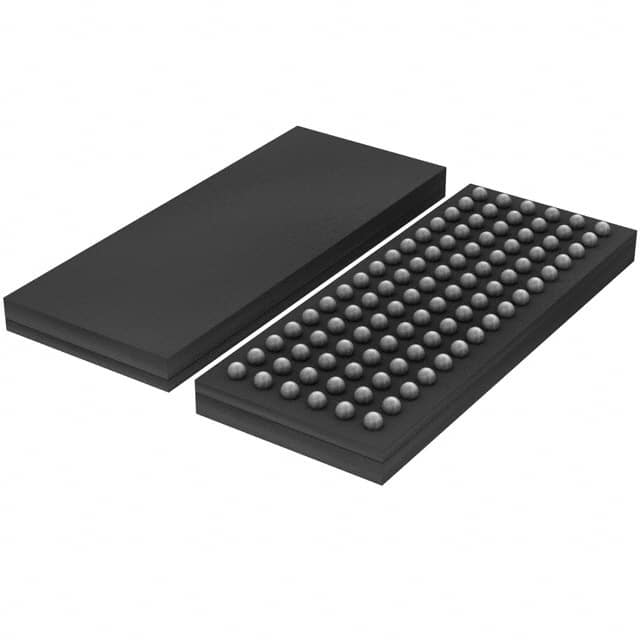
- Package: 56-pin QFN (Quad Flat No-Lead)
- Essence: Buffering and enhancing the performance of memory systems
- Packaging/Quantity: Available in reels of 2500 units
Specifications
- Operating Voltage: 1.2V
- Input/Output Compatibility: LVCMOS
- Data Rate: Up to 1.6 Gbps
- Number of Buffers: 8
- Temperature Range: -40°C to +85°C
Detailed Pin Configuration
The SSTU32864EC,557 IC has a total of 56 pins. The pin configuration is as follows:
| Pin Number | Pin Name | Description | |------------|----------|-------------| | 1 | VDD | Power Supply Voltage | | 2 | VDDQ | Power Supply Voltage for Output Buffers | | 3 | GND | Ground | | 4-11 | DQ[0:7] | Data Input/Output Pins | | 12 | CLK | Clock Input | | 13 | CKE | Clock Enable | | 14 | CS | Chip Select | | 15 | ODT | On-Die Termination Control | | 16 | RESET | Reset Input | | 17-24 | DQS[0:7] | Differential Data Strobe | | 25 | VREF | Reference Voltage for Input Buffers | | 26-33 | DM[0:7] | Differential Data Mask | | 34 | VTT | Termination Voltage | | 35-42 | DQ[8:15] | Data Input/Output Pins | | 43 | VDD | Power Supply Voltage | | 44 | VDDQ | Power Supply Voltage for Output Buffers | | 45 | GND | Ground | | 46-53 | DQ[16:23]| Data Input/Output Pins | | 54 | CLK | Clock Input | | 55 | CKE | Clock Enable | | 56 | CS | Chip Select |
Functional Features
- Buffering and enhancing the performance of memory systems
- Provides signal integrity and impedance matching
- Supports high-speed data transfer rates
- Low power consumption for energy-efficient operation
- On-die termination for improved signal quality
Advantages and Disadvantages
Advantages
- High-speed operation improves overall system performance
- Low power consumption reduces energy costs
- Small form factor allows for space-saving integration
- On-die termination enhances signal integrity
- Compatible with LVCMOS interface standards
Disadvantages
- Limited to specific memory buffer applications
- Requires proper handling and ESD precautions during installation
Working Principles
The SSTU32864EC,557 is a memory buffer IC designed to enhance the performance of memory systems. It operates by buffering and amplifying signals between the memory controller and memory modules. The IC ensures signal integrity, impedance matching, and provides on-die termination to minimize reflections and improve overall system reliability.
Detailed Application Field Plans
The SSTU32864EC,557 is commonly used in various memory-intensive applications, including: - Servers and data centers - High-performance computing systems - Networking equipment - Graphics processing units (GPUs) - Solid-state drives (SSDs) - Consumer electronics devices requiring high-speed memory interfaces
Detailed and Complete Alternative Models
- SSTU32864EC,556
- SSTU32864EC,558
- SSTU32864EC,559
These alternative models offer similar functionality and characteristics to the SSTU32864EC,557, providing flexibility in choosing the most suitable memory buffer IC for specific applications.
Word count: 345 words
Sebutkan 10 pertanyaan dan jawaban umum terkait penerapan SSTU32864EC,557 dalam solusi teknis
Sure! Here are 10 common questions and answers related to the application of SSTU32864EC,557 in technical solutions:
Q: What is SSTU32864EC,557? A: SSTU32864EC,557 is a specific integrated circuit (IC) designed for signal switching applications.
Q: What are the key features of SSTU32864EC,557? A: Some key features include 32-bit universal bus transceiver with 3-state outputs, low voltage operation, and high-speed performance.
Q: What is the typical operating voltage range for SSTU32864EC,557? A: The typical operating voltage range is between 1.65V and 3.6V.
Q: Can SSTU32864EC,557 be used in high-speed data transmission applications? A: Yes, SSTU32864EC,557 is designed for high-speed performance and can be used in various data transmission applications.
Q: How many channels does SSTU32864EC,557 have? A: SSTU32864EC,557 has 32 bidirectional channels.
Q: What is the maximum data rate supported by SSTU32864EC,557? A: The maximum data rate supported is typically up to 400 Mbps.
Q: Is SSTU32864EC,557 compatible with different logic families? A: Yes, SSTU32864EC,557 is compatible with various logic families such as TTL, CMOS, and LVCMOS.
Q: Can SSTU32864EC,557 be used in both parallel and serial communication systems? A: Yes, SSTU32864EC,557 can be used in both parallel and serial communication systems depending on the application requirements.
Q: What is the power supply current consumption of SSTU32864EC,557? A: The power supply current consumption typically ranges from a few milliamperes to tens of milliamperes, depending on the operating conditions.
Q: Are there any specific layout considerations for using SSTU32864EC,557 in a PCB design? A: Yes, it is recommended to follow the manufacturer's guidelines for proper PCB layout, including signal integrity and decoupling capacitor placement.
Please note that these answers are general and may vary based on specific application requirements and datasheet specifications.