

Lihat spesifikasi untuk detail produk.
PDTA124XK,115
Product Overview
Category
PDTA124XK,115 belongs to the category of small signal transistors.
Use
It is commonly used in low-power amplification and switching applications.
Characteristics
- Small form factor
- Low power consumption
- High gain
- Fast switching speed
Package
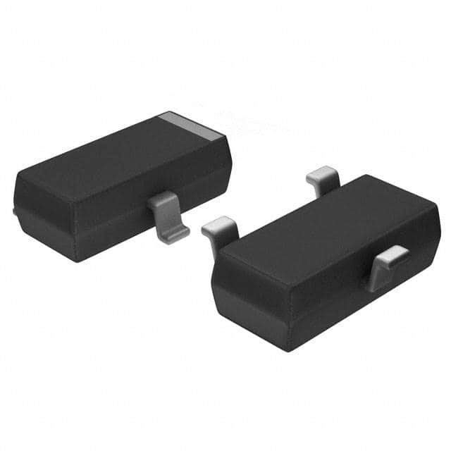
PDTA124XK,115 is typically available in a SOT883 package.
Essence
The essence of PDTA124XK,115 lies in its ability to provide reliable amplification and switching capabilities in compact electronic devices.
Packaging/Quantity
It is usually packaged in reels with a quantity of 3000 units per reel.
Specifications
- Collector-Base Voltage (VCBO): 50V
- Collector-Emitter Voltage (VCEO): 50V
- Emitter-Base Voltage (VEBO): 5V
- Continuous Collector Current (IC): 100mA
- Total Power Dissipation: 200mW
- Transition Frequency (fT): 250MHz
Detailed Pin Configuration
PDTA124XK,115 has the following pin configuration: 1. Base (B) 2. Emitter (E) 3. Collector (C)
Functional Features
- High voltage capability
- Low collector-emitter saturation voltage
- Complementary NPN type available (PDTA124EK,115)
Advantages
- Small size enables use in compact designs
- Low power consumption
- Fast switching speed
Disadvantages
- Limited maximum current handling capability
- Sensitive to overvoltage conditions
Working Principles
PDTA124XK,115 operates based on the principles of bipolar junction transistor (BJT) amplification and switching. When a small current flows into the base terminal, it controls a larger current flow between the collector and emitter terminals, allowing for amplification or switching of signals.
Detailed Application Field Plans
PDTA124XK,115 finds application in various fields including: - Audio amplification circuits - Signal switching in portable electronic devices - Sensor interface circuits - Battery management systems
Detailed and Complete Alternative Models
Some alternative models to PDTA124XK,115 include: - PDTA123EK,115 - PDTA125EK,115 - PDTA126EK,115
In conclusion, PDTA124XK,115 is a small signal transistor with versatile applications in low-power amplification and switching circuits. Its compact size, low power consumption, and fast switching speed make it suitable for integration into modern electronic devices across various industries.
Word count: 366
Sebutkan 10 pertanyaan dan jawaban umum terkait penerapan PDTA124XK,115 dalam solusi teknis
What is PDTA124XK,115?
- PDTA124XK,115 is a high-performance NPN resistor-equipped transistor in a small SOT666 (SC-88) Surface-Mounted Device (SMD) plastic package.
What are the typical applications of PDTA124XK,115?
- Typical applications include high-speed switching and general-purpose amplification in various technical solutions.
What is the maximum collector current of PDTA124XK,115?
- The maximum collector current is 100 mA.
What is the voltage rating for PDTA124XK,115?
- The voltage rating is 50 V.
What are the key features of PDTA124XK,115?
- Some key features include low collector-emitter saturation voltage, high current gain, and low equivalent on-resistance.
Can PDTA124XK,115 be used in audio amplifier circuits?
- Yes, it can be used in audio amplifier circuits due to its general-purpose amplification capabilities.
Is PDTA124XK,115 suitable for high-frequency applications?
- Yes, it is suitable for high-frequency applications due to its high-speed switching characteristics.
What are the thermal characteristics of PDTA124XK,115?
- The thermal resistance from junction to ambient is typically 625 K/W.
Does PDTA124XK,115 require any external components for basic operation?
- No, it does not require any external components for basic operation as it is a complete transistor with built-in resistors.
Are there any recommended PCB layout considerations for using PDTA124XK,115?
- It is recommended to follow standard PCB layout guidelines for SMD components, including proper grounding and minimal trace lengths for high-frequency applications.