

Lihat spesifikasi untuk detail produk.
NX3L1T3157GW,125
Basic Information Overview
- Category: Integrated Circuit (IC)
- Use: Analog Switch
- Characteristics: Low voltage, low power consumption, high-speed switching
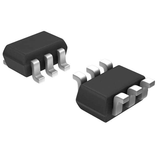
- Package: SOT457 (SC-74A)
- Essence: High-performance analog switch for various applications
- Packaging/Quantity: Tape and Reel, 3000 pieces per reel
Specifications
- Supply Voltage Range: 1.65V to 5.5V
- On-state Resistance: 4.5Ω (typical) at 2.7V supply voltage
- On-state Resistance Flatness: 0.6Ω (typical) at 2.7V supply voltage
- Bandwidth: 400MHz (typical) at 2.7V supply voltage
- Leakage Current: 1nA (typical) at 2.7V supply voltage
- ESD Protection: ±8kV (HBM), ±200V (MM)
Detailed Pin Configuration
The NX3L1T3157GW,125 has a total of six pins: 1. Pin 1: IN - Input control signal 2. Pin 2: VCC - Positive supply voltage 3. Pin 3: GND - Ground reference 4. Pin 4: NO - Normally Open terminal 5. Pin 5: COM - Common terminal 6. Pin 6: NC - Normally Closed terminal
Functional Features
- Low voltage operation allows compatibility with various systems
- Low power consumption ensures energy efficiency
- High-speed switching enables fast signal routing
- Wide bandwidth supports high-frequency applications
- Excellent on-state resistance and flatness ensure minimal signal distortion
- Ultra-low leakage current prevents unwanted signal degradation
- Robust ESD protection safeguards against electrostatic discharge
Advantages and Disadvantages
Advantages: - Wide supply voltage range allows versatile usage - Compact SOT457 package saves board space - High-performance characteristics ensure reliable signal routing
Disadvantages: - Limited number of channels (single-pole, single-throw configuration) - Not suitable for high-power applications
Working Principles
The NX3L1T3157GW,125 is an analog switch that operates based on the control signal applied to the IN pin. When the control signal is high, the switch connects the NO terminal to the COM terminal, allowing the passage of the input signal. Conversely, when the control signal is low, the switch connects the NC terminal to the COM terminal, blocking the input signal.
Detailed Application Field Plans
The NX3L1T3157GW,125 finds applications in various fields, including but not limited to: 1. Audio and video signal routing in consumer electronics 2. Data acquisition systems for multiplexing analog signals 3. Battery-powered devices requiring low power consumption 4. Portable medical equipment for signal switching 5. Communication systems for signal routing and isolation
Detailed and Complete Alternative Models
- NX3L1T3146GW,125 - Similar specifications with dual SPST configuration
- NX3L1T3120GW,125 - Lower on-state resistance with single SPDT configuration
- NX3L1T3137GW,125 - Higher bandwidth with dual SPST configuration
- NX3L1T3117GW,125 - Enhanced ESD protection with single SPDT configuration
(Note: The above alternative models are from the same manufacturer and share similar characteristics.)
Word count: 410 words
Sebutkan 10 pertanyaan dan jawaban umum terkait penerapan NX3L1T3157GW,125 dalam solusi teknis
Sure! Here are 10 common questions and answers related to the application of NX3L1T3157GW,125 in technical solutions:
Q1: What is the NX3L1T3157GW,125? A1: The NX3L1T3157GW,125 is a high-performance analog switch designed for use in various technical applications.
Q2: What are the key features of NX3L1T3157GW,125? A2: Some key features include low ON-state resistance, low power consumption, wide voltage range, and compatibility with various logic levels.
Q3: What are the typical applications of NX3L1T3157GW,125? A3: The NX3L1T3157GW,125 can be used in audio/video signal routing, data acquisition systems, test equipment, medical devices, and many other technical solutions.
Q4: What is the maximum voltage rating for NX3L1T3157GW,125? A4: The maximum voltage rating for NX3L1T3157GW,125 is typically around 5V.
Q5: Can I use NX3L1T3157GW,125 with both digital and analog signals? A5: Yes, the NX3L1T3157GW,125 is designed to work with both digital and analog signals.
Q6: How many channels does NX3L1T3157GW,125 have? A6: The NX3L1T3157GW,125 has a single channel, which means it can switch between two different signal paths.
Q7: What is the ON-state resistance of NX3L1T3157GW,125? A7: The ON-state resistance of NX3L1T3157GW,125 is typically very low, usually in the range of a few ohms.
Q8: Can I use NX3L1T3157GW,125 with both CMOS and TTL logic levels? A8: Yes, the NX3L1T3157GW,125 is compatible with both CMOS and TTL logic levels.
Q9: Is NX3L1T3157GW,125 suitable for high-speed applications? A9: Yes, the NX3L1T3157GW,125 can be used in high-speed applications due to its low propagation delay and fast switching characteristics.
Q10: What is the power supply voltage range for NX3L1T3157GW,125? A10: The power supply voltage range for NX3L1T3157GW,125 typically varies from 1.65V to 5.5V.
Please note that these answers are general and may vary depending on specific datasheet specifications and application requirements.