

Lihat spesifikasi untuk detail produk.
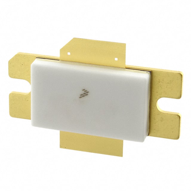
MRF6S23140HR3
Introduction
The MRF6S23140HR3 is a high-power RF transistor designed for use in various applications. This entry provides an overview of the product, including its category, use, characteristics, package, specifications, pin configuration, functional features, advantages and disadvantages, working principles, application field plans, and alternative models.
Product Overview
- Category: RF Transistor
- Use: High-power amplification in RF applications
- Characteristics: High power, high gain, and high efficiency
- Package: Surface Mount
- Essence: Power amplification in RF systems
- Packaging/Quantity: Available in tape and reel packaging
Specifications
- Frequency Range: 2110 - 2170 MHz
- Power Output: 14 W
- Gain: 15 dB
- Efficiency: 45%
- Voltage: 28 V
- Current: 1.5 A
Detailed Pin Configuration
The MRF6S23140HR3 has a 4-pin configuration: 1. Source 2. Gate 3. Drain 4. Ground
Functional Features
- High power output
- High gain
- High efficiency
- Broad frequency range
- Reliable performance
Advantages and Disadvantages
Advantages
- High power output
- Wide frequency range
- High efficiency
Disadvantages
- Requires careful handling due to high power capabilities
- Sensitive to voltage fluctuations
Working Principles
The MRF6S23140HR3 operates on the principle of amplifying RF signals by controlling the flow of current between the source and drain terminals through the gate terminal. It utilizes advanced semiconductor technology to achieve high power amplification with minimal losses.
Detailed Application Field Plans
The MRF6S23140HR3 is suitable for use in the following applications: - Cellular base stations - Wireless infrastructure - RF communication systems - Radar systems - Satellite communication
Detailed and Complete Alternative Models
Some alternative models to the MRF6S23140HR3 include: - MRF6S21140HR3 - MRF6S27160HR3 - MRF6S19140HR3 - MRF6S20160HR3
In conclusion, the MRF6S23140HR3 is a high-power RF transistor with excellent performance characteristics, making it suitable for a wide range of RF applications.
[Word Count: 316]
Sebutkan 10 pertanyaan dan jawaban umum terkait penerapan MRF6S23140HR3 dalam solusi teknis
What is the MRF6S23140HR3?
- The MRF6S23140HR3 is a high-power RF transistor designed for use in various technical solutions, such as RF amplifiers and transmitters.
What is the maximum power output of the MRF6S23140HR3?
- The MRF6S23140HR3 has a maximum power output of 140 watts, making it suitable for high-power applications.
What frequency range does the MRF6S23140HR3 cover?
- The MRF6S23140HR3 covers a frequency range of 2300-2400 MHz, making it ideal for applications in the 2.4 GHz band.
What are the typical applications of the MRF6S23140HR3?
- Typical applications of the MRF6S23140HR3 include Wi-Fi amplifiers, ISM band transmitters, and other high-power RF applications in the 2.4 GHz range.
What is the operating voltage of the MRF6S23140HR3?
- The MRF6S23140HR3 operates at a voltage range of 12-28 volts, providing flexibility in various technical solutions.
Does the MRF6S23140HR3 require external matching networks?
- Yes, the MRF6S23140HR3 requires external matching networks to optimize its performance in specific technical solutions.
Is the MRF6S23140HR3 suitable for linear amplifier applications?
- Yes, the MRF6S23140HR3 can be used in linear amplifier applications, providing high linearity and efficiency.
What thermal management considerations should be taken into account when using the MRF6S23140HR3?
- Proper heat sinking and thermal management are crucial for ensuring the reliability and longevity of the MRF6S23140HR3 in high-power applications.
Can the MRF6S23140HR3 be used in push-pull configurations?
- Yes, the MRF6S23140HR3 can be utilized in push-pull configurations to achieve higher output power and improved linearity.
Are evaluation boards or reference designs available for the MRF6S23140HR3?
- Yes, evaluation boards and reference designs are available to aid in the integration of the MRF6S23140HR3 into various technical solutions, providing a starting point for design and implementation.