

Lihat spesifikasi untuk detail produk.
74LV139BQ,115
Basic Information Overview
- Category: Integrated Circuit (IC)
- Use: Decoder/Demultiplexer
- Characteristics: Low-voltage, dual 2-to-4 line decoder/demultiplexer
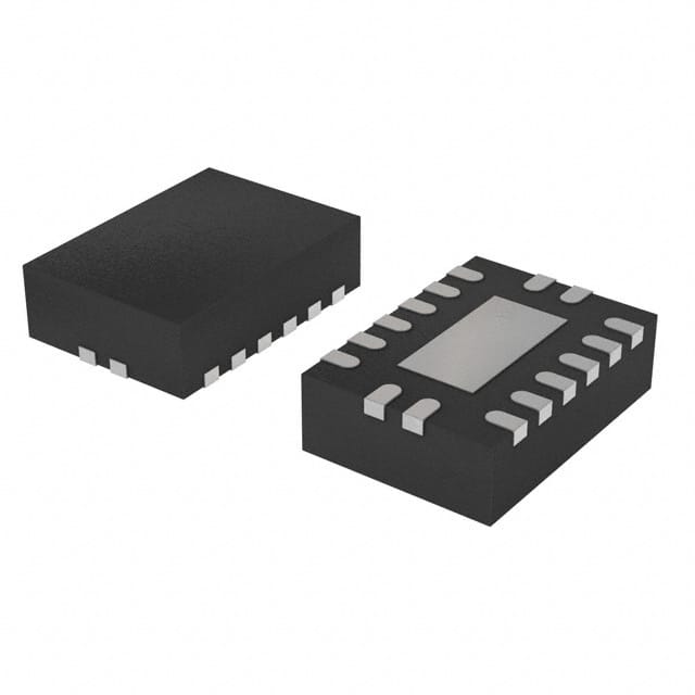
- Package: BGA (Ball Grid Array)
- Essence: Logic IC for decoding and demultiplexing signals
- Packaging/Quantity: Tape and Reel, 2500 units per reel
Specifications
- Supply Voltage Range: 1.65V to 5.5V
- Input Voltage Range: -0.5V to VCC + 0.5V
- Output Voltage Range: 0V to VCC
- Maximum Operating Frequency: 125 MHz
- Number of Inputs: 2
- Number of Outputs: 4
- Propagation Delay Time: 6 ns (typical)
Detailed Pin Configuration
The 74LV139BQ,115 has a total of 16 pins. The pin configuration is as follows:
Pin 1: GND (Ground)
Pin 2: A0 (Input A0)
Pin 3: A1 (Input A1)
Pin 4: Y0 (Output Y0)
Pin 5: Y1 (Output Y1)
Pin 6: Y2 (Output Y2)
Pin 7: Y3 (Output Y3)
Pin 8: GND (Ground)
Pin 9: E1 (Enable Input 1)
Pin 10: E2 (Enable Input 2)
Pin 11: VCC (Supply Voltage)
Pin 12: B0 (Input B0)
Pin 13: B1 (Input B1)
Pin 14: Y4 (Output Y4)
Pin 15: Y5 (Output Y5)
Pin 16: Y6 (Output Y6)
Functional Features
- Dual 2-to-4 line decoder/demultiplexer functionality
- Low-voltage operation suitable for battery-powered devices
- High-speed operation with low propagation delay time
- Enable inputs for easy control of decoding/demultiplexing
Advantages and Disadvantages
Advantages: - Low-voltage operation allows for compatibility with various systems - High-speed operation enables quick signal decoding/demultiplexing - Small package size saves board space - Enable inputs provide flexibility in controlling the device
Disadvantages: - Limited number of inputs and outputs may not be suitable for complex applications - BGA package may require specialized equipment for soldering/rework
Working Principles
The 74LV139BQ,115 is a dual 2-to-4 line decoder/demultiplexer IC. It takes two input lines (A0 and A1) and two enable inputs (E1 and E2) to decode and demultiplex the input signals. The outputs (Y0 to Y6) correspond to different combinations of the input lines. When the enable inputs are active, the selected output line becomes active based on the input combination.
Detailed Application Field Plans
The 74LV139BQ,115 can be used in various applications, including: - Address decoding in microcontrollers and microprocessors - Data routing in communication systems - Signal demultiplexing in digital circuits - Control logic in industrial automation systems - Function selection in electronic devices
Detailed and Complete Alternative Models
Some alternative models that offer similar functionality to the 74LV139BQ,115 include: - SN74LS139N: Dual 2-to-4 line decoder/demultiplexer by Texas Instruments - CD74HC139E: High-speed CMOS logic dual 2-to-4 line decoder/demultiplexer by Texas Instruments - MC74HC139AN: Dual 2-to-4 line decoder/demultiplexer by ON Semiconductor
These alternative models can be considered based on specific requirements and availability.
Word count: 346 words
Sebutkan 10 pertanyaan dan jawaban umum terkait penerapan 74LV139BQ,115 dalam solusi teknis
Sure! Here are 10 common questions and answers related to the application of 74LV139BQ,115 in technical solutions:
Question: What is the function of the 74LV139BQ,115?
Answer: The 74LV139BQ,115 is a dual 2-to-4 line decoder/demultiplexer IC that can be used to decode binary information and control multiple outputs.Question: What is the operating voltage range for the 74LV139BQ,115?
Answer: The 74LV139BQ,115 operates within a voltage range of 1.65V to 5.5V.Question: How many inputs does the 74LV139BQ,115 have?
Answer: The 74LV139BQ,115 has two 2-inputs (A0, A1) for decoding purposes.Question: How many outputs does the 74LV139BQ,115 have?
Answer: The 74LV139BQ,115 has four outputs (Y0, Y1, Y2, Y3) that can be controlled based on the input signals.Question: Can the 74LV139BQ,115 be used as a demultiplexer?
Answer: Yes, the 74LV139BQ,115 can be used as a demultiplexer by connecting the appropriate inputs and using the outputs to select different channels.Question: What is the maximum frequency at which the 74LV139BQ,115 can operate?
Answer: The 74LV139BQ,115 can operate at a maximum frequency of 125 MHz.Question: Is the 74LV139BQ,115 compatible with TTL logic levels?
Answer: Yes, the 74LV139BQ,115 is compatible with TTL logic levels and can be used in mixed logic systems.Question: Can the 74LV139BQ,115 be cascaded to increase the number of outputs?
Answer: Yes, multiple 74LV139BQ,115 ICs can be cascaded together to increase the number of outputs and decode more complex binary patterns.Question: What is the power consumption of the 74LV139BQ,115?
Answer: The power consumption of the 74LV139BQ,115 is typically low, making it suitable for battery-powered applications.Question: Are there any specific application examples for the 74LV139BQ,115?
Answer: Yes, the 74LV139BQ,115 can be used in various applications such as address decoding, data routing, memory selection, and general-purpose digital logic circuits.
Please note that these answers are general and may vary depending on the specific requirements and implementation of the 74LV139BQ,115 in a technical solution.