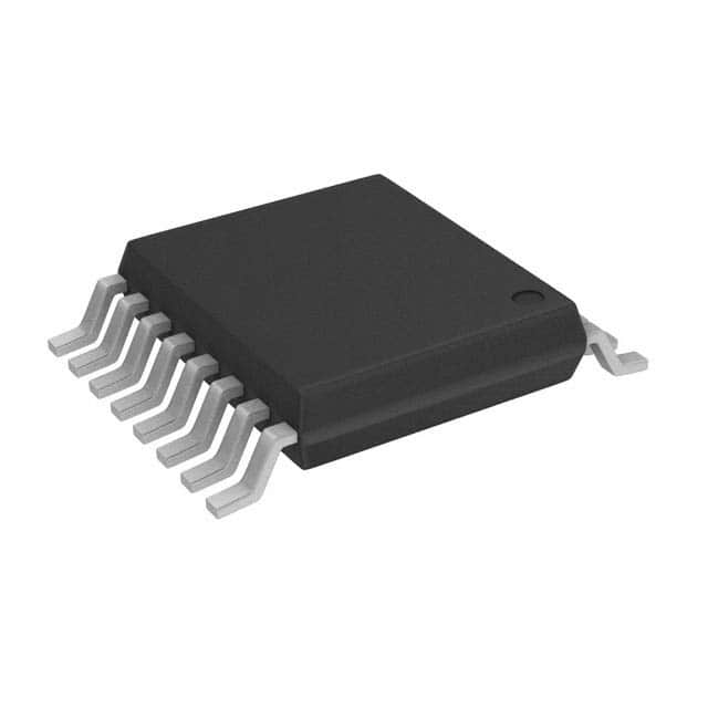
Lihat spesifikasi untuk detail produk.

74HC283PW,118
Product Overview
- Category: Integrated Circuit (IC)
- Use: Arithmetic Logic Unit (ALU)
- Characteristics: High-speed operation, low power consumption
- Package: TSSOP (Thin Shrink Small Outline Package)
- Essence: 4-bit binary full adder
- Packaging/Quantity: Tape and reel, 2500 units per reel
Specifications
- Supply Voltage Range: 2 V to 6 V
- Input Voltage Range: 0 V to VCC
- Operating Temperature Range: -40°C to +125°C
- Propagation Delay: 10 ns (typical)
- Power Dissipation: 500 mW (max)
Pin Configuration
The 74HC283PW,118 has a total of 16 pins. The pin configuration is as follows:
- A3 (Input)
- B3 (Input)
- A2 (Input)
- B2 (Input)
- A1 (Input)
- B1 (Input)
- A0 (Input)
- B0 (Input)
- CIN (Input)
- GND (Ground)
- S (Sum Output)
- COUT (Carry Output)
- P (Parity Output)
- LT (Less Than Output)
- G1 (Gate 1 Input)
- VCC (Supply Voltage)
Functional Features
- Performs addition of two 4-bit binary numbers
- Generates sum output (S), carry output (COUT), parity output (P), and less than output (LT)
- Supports cascading for larger bit-width addition operations
- Provides high-speed operation with minimal power consumption
Advantages and Disadvantages
Advantages: - High-speed operation allows for efficient arithmetic calculations - Low power consumption reduces energy requirements - Compact TSSOP package enables space-saving designs
Disadvantages: - Limited to 4-bit addition operations, not suitable for larger bit-width calculations - Requires external circuitry for handling carry propagation in multi-bit additions
Working Principles
The 74HC283PW,118 is a 4-bit binary full adder integrated circuit. It performs addition of two 4-bit binary numbers by generating the sum output (S), carry output (COUT), parity output (P), and less than output (LT). The inputs A3-A0 and B3-B0 represent the binary numbers to be added, while the CIN input allows for cascading multiple ICs for larger bit-width addition operations.
The internal circuitry of the 74HC283PW,118 utilizes logic gates and flip-flops to perform the addition operation. The carry propagation is handled by the CIN input and the carry output (COUT) is generated accordingly. The sum output (S) represents the result of the addition, while the parity output (P) indicates whether the number of set bits in the sum is even or odd. The less than output (LT) determines if the sum is less than the reference value.
Detailed Application Field Plans
The 74HC283PW,118 is commonly used in various applications that require arithmetic calculations, such as:
- Microcontrollers: Used in microcontroller-based systems for performing mathematical operations.
- Digital Signal Processing: Employed in digital signal processing circuits for efficient data manipulation.
- Communication Systems: Integrated into communication systems for encoding and decoding operations.
- Computer Arithmetic Units: Utilized in computer arithmetic units for adding binary numbers.
- Industrial Control Systems: Incorporated in industrial control systems for precise calculations.
Detailed and Complete Alternative Models
Some alternative models to the 74HC283PW,118 include:
- SN74LS283N: 4-bit binary full adder with similar specifications and pin configuration.
- CD74HC283E: High-speed CMOS logic IC with 4-bit binary addition capabilities.
- MC74HC283ADR2G: 4-bit binary full adder in SOIC (Small Outline Integrated Circuit) package.
These alternative models offer similar functionality and can be used as substitutes depending on specific requirements.
Word count: 530 words
Sebutkan 10 pertanyaan dan jawaban umum terkait penerapan 74HC283PW,118 dalam solusi teknis
Sure! Here are 10 common questions and answers related to the application of 74HC283PW,118 in technical solutions:
Q: What is the 74HC283PW,118? A: The 74HC283PW,118 is a 4-bit binary full adder integrated circuit (IC) that can perform addition of two 4-bit numbers.
Q: What is the operating voltage range for the 74HC283PW,118? A: The operating voltage range for the 74HC283PW,118 is typically between 2V and 6V.
Q: How many inputs does the 74HC283PW,118 have? A: The 74HC283PW,118 has eight inputs - four inputs for each 4-bit number being added.
Q: What is the output format of the 74HC283PW,118? A: The 74HC283PW,118 provides a 4-bit sum output and a carry-out output.
Q: Can the 74HC283PW,118 be cascaded to add larger numbers? A: Yes, multiple 74HC283PW,118 ICs can be cascaded together to add larger numbers by connecting the carry-out of one IC to the carry-in of the next.
Q: What is the maximum clock frequency supported by the 74HC283PW,118? A: The maximum clock frequency supported by the 74HC283PW,118 is typically around 50 MHz.
Q: Does the 74HC283PW,118 have any built-in error detection or correction features? A: No, the 74HC283PW,118 does not have any built-in error detection or correction features. It performs basic binary addition.
Q: Can the 74HC283PW,118 be used in both digital and analog circuits? A: No, the 74HC283PW,118 is specifically designed for digital applications and should not be used in analog circuits.
Q: What is the power consumption of the 74HC283PW,118? A: The power consumption of the 74HC283PW,118 is typically low, making it suitable for battery-powered devices.
Q: Are there any recommended external components to use with the 74HC283PW,118? A: It is generally recommended to use decoupling capacitors near the power supply pins of the IC to ensure stable operation.
Please note that these answers are general and may vary depending on specific datasheet specifications and application requirements.

