

Lihat spesifikasi untuk detail produk.
Encyclopedia Entry: 74ABT544DB,112
Product Overview
Category
The 74ABT544DB,112 belongs to the category of integrated circuits (ICs).
Use
This IC is commonly used in digital electronic systems for signal amplification and buffering purposes.
Characteristics
- High-speed operation
- Low power consumption
- Wide operating voltage range
- Schmitt-trigger inputs for noise immunity
- Output drive capability: ±24 mA at VCC = 5V
Package
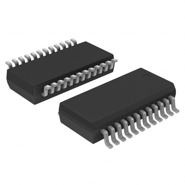
The 74ABT544DB,112 is available in a standard 20-pin SSOP (Shrink Small Outline Package) package.
Essence
The essence of this product lies in its ability to provide reliable signal amplification and buffering in digital electronic systems.
Packaging/Quantity
The 74ABT544DB,112 is typically packaged in reels or tubes, with a quantity of 250 units per reel/tube.
Specifications
- Supply Voltage Range: 4.5V to 5.5V
- Input Voltage Range: 0V to VCC
- Operating Temperature Range: -40°C to +85°C
- Propagation Delay Time: 3.5 ns (max)
- Output Current: ±24 mA
Detailed Pin Configuration
The 74ABT544DB,112 has a total of 20 pins, which are assigned specific functions as follows:
- Pin 1: Output Enable (OE)
- Pin 2: Data Input D0
- Pin 3: Data Input D1
- Pin 4: Data Input D2
- Pin 5: Data Input D3
- Pin 6: Data Input D4
- Pin 7: Data Input D5
- Pin 8: Data Input D6
- Pin 9: Data Input D7
- Pin 10: GND (Ground)
- Pin 11: Data Output Q0
- Pin 12: Data Output Q1
- Pin 13: Data Output Q2
- Pin 14: Data Output Q3
- Pin 15: Data Output Q4
- Pin 16: Data Output Q5
- Pin 17: Data Output Q6
- Pin 18: Data Output Q7
- Pin 19: VCC (Supply Voltage)
- Pin 20: Output Enable (OE)
Functional Features
The 74ABT544DB,112 is designed to provide bidirectional signal amplification and buffering. It features a high-speed operation, low power consumption, and wide operating voltage range. The Schmitt-trigger inputs ensure noise immunity, making it suitable for applications in noisy environments.
Advantages and Disadvantages
Advantages
- High-speed operation allows for efficient signal processing.
- Low power consumption helps in reducing overall system power requirements.
- Wide operating voltage range provides flexibility in different electronic systems.
- Schmitt-trigger inputs enhance noise immunity, ensuring reliable signal transmission.
Disadvantages
- Limited output drive capability may restrict its use in certain high-current applications.
- The SSOP package may require careful handling during assembly to avoid damage.
Working Principles
The 74ABT544DB,112 operates based on the principles of digital logic. It receives input signals through the data input pins (D0-D7) and amplifies/buffers them as per the control signals provided by the output enable pins (OE). The amplified/buffered signals are then available at the corresponding data output pins (Q0-Q7).
Detailed Application Field Plans
The 74ABT544DB,112 finds applications in various digital electronic systems, including but not limited to: - Microcontrollers - Data communication systems - Memory modules - Industrial automation equipment - Automotive electronics
Detailed and Complete Alternative Models
Some alternative models that offer similar functionality to the 74ABT544DB,112 include: - SN74ABT544A by Texas Instruments - MC74ABT544DW by ON Semiconductor - CD74ABT544M by Texas Instruments - 74ABT544D by NXP Semiconductors
These alternative models can be considered based on specific requirements and availability.
Word count: 489 words
Sebutkan 10 pertanyaan dan jawaban umum terkait penerapan 74ABT544DB,112 dalam solusi teknis
Sure! Here are 10 common questions and answers related to the application of 74ABT544DB,112 in technical solutions:
Q: What is the function of the 74ABT544DB,112? A: The 74ABT544DB,112 is an octal registered transceiver with tri-state outputs. It can be used for bidirectional data transfer between two buses.
Q: What is the maximum operating voltage for the 74ABT544DB,112? A: The maximum operating voltage for the 74ABT544DB,112 is 5.5V.
Q: Can the 74ABT544DB,112 handle both TTL and CMOS input levels? A: Yes, the 74ABT544DB,112 is compatible with both TTL and CMOS input levels.
Q: How many data inputs and outputs does the 74ABT544DB,112 have? A: The 74ABT544DB,112 has 8 data inputs and 8 data outputs.
Q: Does the 74ABT544DB,112 support bus hold functionality? A: Yes, the 74ABT544DB,112 supports bus hold functionality, which helps to maintain the last valid logic level during bus transitions.
Q: What is the propagation delay of the 74ABT544DB,112? A: The propagation delay of the 74ABT544DB,112 is typically around 4.5 ns.
Q: Can the 74ABT544DB,112 be used in high-speed applications? A: Yes, the 74ABT544DB,112 is designed for high-speed operation and can be used in applications with fast data transfer requirements.
Q: Does the 74ABT544DB,112 have internal pull-up or pull-down resistors? A: No, the 74ABT544DB,112 does not have internal pull-up or pull-down resistors.
Q: Can the 74ABT544DB,112 be used in a multi-master system? A: Yes, the 74ABT544DB,112 can be used in multi-master systems as it supports bidirectional data transfer.
Q: What is the power supply range for the 74ABT544DB,112? A: The power supply range for the 74ABT544DB,112 is typically between 4.5V and 5.5V.
Please note that the answers provided here are general and may vary depending on the specific datasheet and manufacturer's specifications of the 74ABT544DB,112.