

Lihat spesifikasi untuk detail produk.
2N5551,412
Product Overview
The 2N5551,412 is a bipolar junction transistor (BJT) belonging to the category of electronic components. It is commonly used in amplification and switching applications due to its versatile characteristics. The 2N5551,412 is available in a variety of packages and quantities, making it suitable for a wide range of electronic designs.
Basic Information
- Category: Electronic Components
- Use: Amplification and Switching
- Characteristics: High gain, low noise, and reliable performance
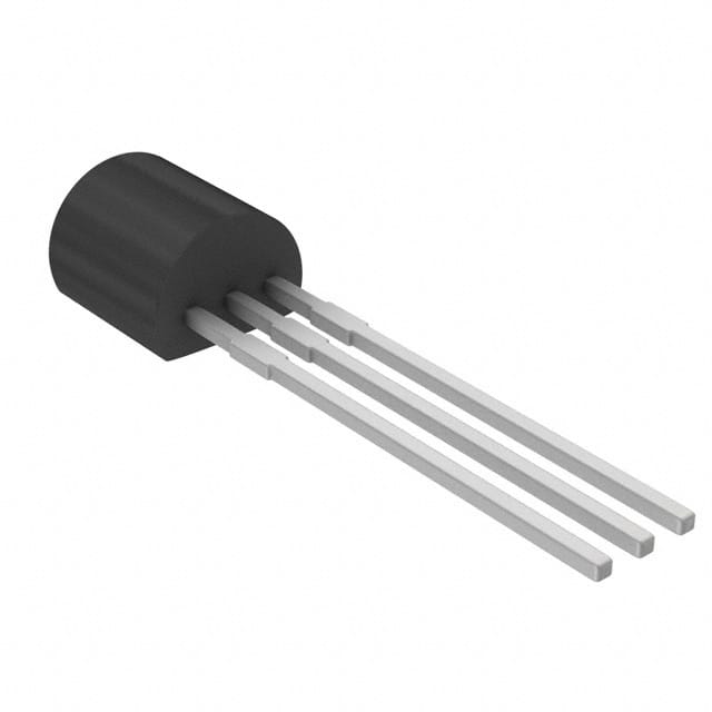
- Package: TO-92, SOT-23
- Essence: NPN BJT
- Packaging/Quantity: Tape & Reel, Bulk
Specifications
The 2N5551,412 features the following specifications: - Collector-Base Voltage (VCBO): 160V - Collector-Emitter Voltage (VCEO): 160V - Emitter-Base Voltage (VEBO): 6V - Collector Current (IC): 600mA - Power Dissipation (PD): 625mW - Transition Frequency (fT): 150MHz
Detailed Pin Configuration
The 2N5551,412 has a standard pin configuration with three terminals: the emitter, base, and collector. The pinout is as follows: - Emitter (E) - Base (B) - Collector (C)
Functional Features
The 2N5551,412 offers the following functional features: - High Gain: Provides significant amplification of input signals. - Low Noise: Minimizes unwanted signal interference. - Reliable Performance: Ensures stable operation over extended periods.
Advantages and Disadvantages
Advantages
- Versatile Application: Suitable for a wide range of electronic circuits.
- High Gain: Enables effective signal amplification.
- Compact Package: Available in small form factors for space-constrained designs.
Disadvantages
- Limited Power Handling: Not suitable for high-power applications.
- Sensitivity to Temperature: Performance may vary with temperature changes.
Working Principles
The 2N5551,412 operates based on the principles of current amplification and control. When a small current flows into the base terminal, it controls a larger current flow between the collector and emitter, allowing for signal amplification or switching.
Detailed Application Field Plans
The 2N5551,412 finds extensive use in various electronic applications, including: - Audio Amplifiers - Signal Processing Circuits - Switching Circuits - Oscillator Circuits - Sensor Interfaces
Detailed and Complete Alternative Models
Several alternative models to the 2N5551,412 include: - BC547 - 2N3904 - 2N2222 - BC548 - 2N4401
In conclusion, the 2N5551,412 is a versatile and widely used BJT that offers high gain and reliable performance in amplification and switching applications. Its compact package and availability in different quantities make it a popular choice for electronic circuit designs.
[Word Count: 414]
Sebutkan 10 pertanyaan dan jawaban umum terkait penerapan 2N5551,412 dalam solusi teknis
What is the 2N5551,412 transistor used for?
- The 2N5551 and 2N412 are general-purpose transistors commonly used in amplification and switching applications.
What are the typical operating conditions for the 2N5551,412 transistors?
- The typical operating conditions for these transistors include a maximum collector current of 600mA, a maximum collector-emitter voltage of 160V, and a maximum power dissipation of 625mW.
How do I identify the pinout of the 2N5551,412 transistors?
- The pinout for these transistors is typically Emitter (E), Base (B), and Collector (C).
Can the 2N5551,412 transistors be used for audio amplification?
- Yes, these transistors can be used for small-signal audio amplification due to their low noise and high gain characteristics.
What are some common circuit configurations using the 2N5551,412 transistors?
- Common circuit configurations include common emitter, common base, and common collector configurations for various amplification and switching purposes.
Are there any specific considerations for driving inductive loads with the 2N5551,412 transistors?
- When driving inductive loads, it's important to use appropriate flyback diodes to protect the transistors from voltage spikes generated by the inductive load.
What are the typical gain values for the 2N5551,412 transistors?
- The typical DC current gain (hFE) for these transistors ranges from 100 to 300, depending on the specific part number and operating conditions.
Can the 2N5551,412 transistors be used in high-frequency applications?
- While these transistors have limited high-frequency performance, they can still be used in low-to-moderate frequency applications such as audio amplification and general-purpose switching.
What are the storage and operating temperature ranges for the 2N5551,412 transistors?
- The storage temperature range is typically -65°C to +150°C, while the operating temperature range is usually -55°C to +150°C.
Are there any recommended heat sinking or thermal management considerations for the 2N5551,412 transistors?
- For high-power or high-temperature applications, proper heat sinking and thermal management should be employed to ensure the transistors operate within their specified temperature limits.