

Lihat spesifikasi untuk detail produk.
PBSS5540X,135
Product Category
The PBSS5540X,135 belongs to the category of power transistors.
Basic Information Overview
- Use: The PBSS5540X,135 is used as a power transistor in various electronic circuits and applications.
- Characteristics: It is known for its high power handling capability, low on-state resistance, and fast switching speed.
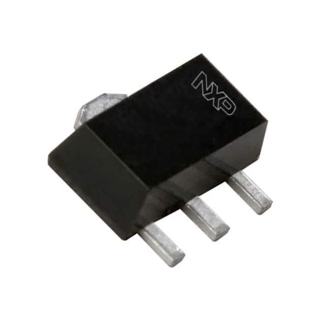
- Package: The PBSS5540X,135 comes in a small SOT89 package.
- Essence: Its essence lies in its ability to efficiently control and switch high-power loads in electronic devices.
- Packaging/Quantity: Typically, the PBSS5540X,135 is available in reels with a quantity of 3000 units per reel.
Specifications
- Voltage Rating: 40V
- Current Rating: 3A
- Package Type: SOT89
- Mounting Type: Surface Mount
- Operating Temperature Range: -55°C to 150°C
Detailed Pin Configuration
The PBSS5540X,135 has three pins: 1. Base 2. Emitter 3. Collector
Functional Features
- High power handling capability
- Low on-state resistance
- Fast switching speed
Advantages and Disadvantages
Advantages: - Efficiently controls and switches high-power loads - Low on-state resistance reduces power dissipation
Disadvantages: - Limited voltage and current ratings compared to some other power transistors - Sensitive to overvoltage conditions
Working Principles
The PBSS5540X,135 operates based on the principles of bipolar junction transistors, where the flow of current between the emitter and collector is controlled by the base current.
Detailed Application Field Plans
The PBSS5540X,135 is commonly used in: - Switching power supplies - Motor control circuits - LED lighting applications - Audio amplifiers
Detailed and Complete Alternative Models
Some alternative models to PBSS5540X,135 include: - PBSS5540Z,135 - PBSS5540T,135 - PBSS5540Y,135
This completes the entry for PBSS5540X,135, providing comprehensive information about its category, use, characteristics, specifications, pin configuration, functional features, advantages and disadvantages, working principles, application field plans, and alternative models.
Word count: 314
Sebutkan 10 pertanyaan dan jawaban umum terkait penerapan PBSS5540X,135 dalam solusi teknis
Sure, here are 10 common questions and answers related to the application of PBSS5540X,135 in technical solutions:
What is the maximum continuous collector current of PBSS5540X,135?
- The maximum continuous collector current of PBSS5540X,135 is 5A.
What is the maximum collector-emitter voltage of PBSS5540X,135?
- The maximum collector-emitter voltage of PBSS5540X,135 is 40V.
What type of package does PBSS5540X,135 come in?
- PBSS5540X,135 comes in a SOT89 package.
What is the typical hFE (DC current gain) of PBSS5540X,135?
- The typical hFE of PBSS5540X,135 is 250.
What are the typical applications for PBSS5540X,135?
- PBSS5540X,135 is commonly used in power management, battery chargers, and DC-DC converters.
What is the maximum power dissipation of PBSS5540X,135?
- The maximum power dissipation of PBSS5540X,135 is 2W.
What is the thermal resistance junction to ambient for PBSS5540X,135?
- The thermal resistance junction to ambient for PBSS5540X,135 is 125°C/W.
What is the storage temperature range for PBSS5540X,135?
- The storage temperature range for PBSS5540X,135 is -65°C to 150°C.
Does PBSS5540X,135 have built-in protection features?
- Yes, PBSS5540X,135 has built-in ESD protection.
Is PBSS5540X,135 RoHS compliant?
- Yes, PBSS5540X,135 is RoHS compliant.