

Lihat spesifikasi untuk detail produk.
Encyclopedia Entry: 74VHCT595BQ-Q100X
Product Overview
- Category: Integrated Circuit (IC)
- Use: Shift Register
- Characteristics: High-Speed, Low-Power, CMOS Technology
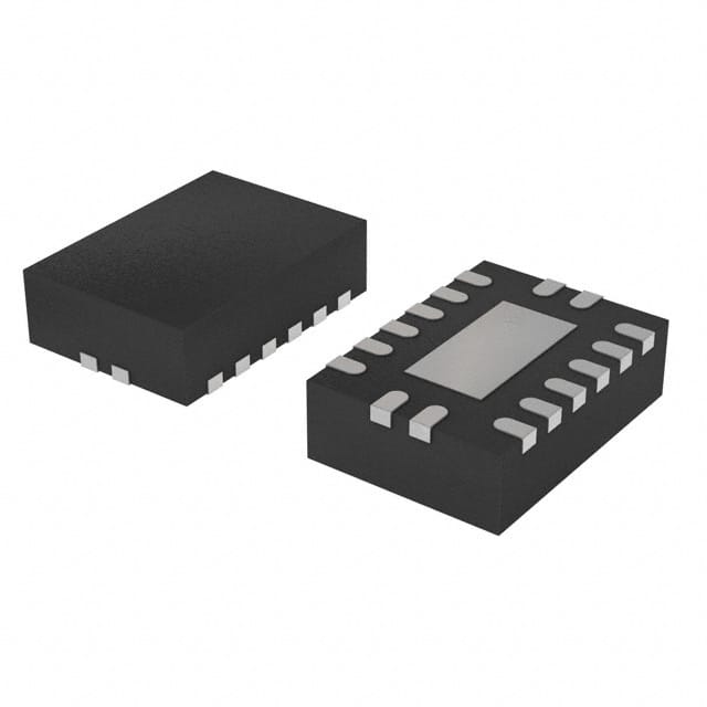
- Package: QFN (Quad Flat No-Lead)
- Essence: Serial-In, Parallel-Out Shift Register
- Packaging/Quantity: Tape and Reel, 2500 pieces per reel
Specifications
- Supply Voltage: 2.0V to 5.5V
- Input Voltage: 0V to VCC
- Output Voltage: 0V to VCC
- Operating Temperature Range: -40°C to +125°C
- Maximum Clock Frequency: 74 MHz
- Number of Stages: 8
- Output Type: Tri-State
Detailed Pin Configuration
The 74VHCT595BQ-Q100X IC has a total of 16 pins, which are assigned specific functions as follows:
- SER (Serial Data Input)
- QA (Parallel Output A)
- QB (Parallel Output B)
- QC (Parallel Output C)
- QD (Parallel Output D)
- QE (Parallel Output E)
- QF (Parallel Output F)
- QG (Parallel Output G)
- GND (Ground)
- QH' (Parallel Output H')
- MR (Master Reset)
- SH_CP (Shift Register Clock Input)
- ST_CP (Storage Register Clock Input)
- OE (Output Enable)
- DS (Serial Data Output)
- VCC (Supply Voltage)
Functional Features
- Serial-in, parallel-out shift register with an 8-bit storage register
- High-speed operation with a maximum clock frequency of 74 MHz
- Low-power consumption due to CMOS technology
- Tri-state outputs for easy interfacing with other devices
- Master reset function for clearing the shift and storage registers
- Output enable control for disabling the outputs when not required
Advantages and Disadvantages
Advantages: - High-speed operation allows for efficient data transfer - Low-power consumption makes it suitable for battery-powered applications - Tri-state outputs facilitate easy integration with other components - Compact QFN package saves board space
Disadvantages: - Limited number of stages (8) may not be sufficient for certain applications requiring larger shift registers - Lack of built-in error detection or correction mechanisms
Working Principles
The 74VHCT595BQ-Q100X is a serial-in, parallel-out shift register. It receives data serially through the SER pin and shifts it into the internal shift register on each rising edge of the shift register clock (SHCP). The data can then be transferred to the parallel output pins (QA-QH') by activating the storage register clock (STCP). The outputs can be enabled or disabled using the output enable (OE) pin.
Detailed Application Field Plans
The 74VHCT595BQ-Q100X IC finds applications in various fields, including: 1. Data communication systems 2. Industrial automation 3. Automotive electronics 4. Consumer electronics 5. Robotics 6. LED displays 7. Instrumentation
Detailed and Complete Alternative Models
Some alternative models that offer similar functionality to the 74VHCT595BQ-Q100X IC include: 1. SN74HC595 - Texas Instruments 2. CD4094 - Texas Instruments 3. 74HC595 - NXP Semiconductors 4. M74HC595 - STMicroelectronics 5. MC74HC595A - ON Semiconductor
Note: This encyclopedia entry provides an overview of the 74VHCT595BQ-Q100X IC, including its basic information, specifications, pin configuration, functional features, advantages and disadvantages, working principles, application field plans, and alternative models.
Sebutkan 10 pertanyaan dan jawaban umum terkait penerapan 74VHCT595BQ-Q100X dalam solusi teknis
Sure! Here are 10 common questions and answers related to the application of 74VHCT595BQ-Q100X in technical solutions:
Question: What is the purpose of the 74VHCT595BQ-Q100X?
Answer: The 74VHCT595BQ-Q100X is an 8-bit shift register with output latches, commonly used for serial-to-parallel data conversion.Question: What is the operating voltage range of the 74VHCT595BQ-Q100X?
Answer: The 74VHCT595BQ-Q100X operates within a voltage range of 4.5V to 5.5V.Question: How many outputs does the 74VHCT595BQ-Q100X have?
Answer: The 74VHCT595BQ-Q100X has 8 outputs, each capable of driving standard TTL loads.Question: Can the 74VHCT595BQ-Q100X be cascaded to increase the number of outputs?
Answer: Yes, multiple 74VHCT595BQ-Q100X devices can be cascaded together to expand the number of outputs.Question: What is the maximum clock frequency supported by the 74VHCT595BQ-Q100X?
Answer: The 74VHCT595BQ-Q100X can operate at a maximum clock frequency of 25 MHz.Question: Does the 74VHCT595BQ-Q100X have any built-in protection features?
Answer: Yes, the 74VHCT595BQ-Q100X includes input diodes that provide protection against electrostatic discharge (ESD).Question: Can the 74VHCT595BQ-Q100X be used in both parallel and serial data transfer modes?
Answer: Yes, the 74VHCT595BQ-Q100X supports both parallel and serial data transfer modes, making it versatile for various applications.Question: What is the power consumption of the 74VHCT595BQ-Q100X?
Answer: The power consumption of the 74VHCT595BQ-Q100X is typically low, making it suitable for battery-powered devices.Question: Does the 74VHCT595BQ-Q100X have any special features for reducing noise?
Answer: Yes, the 74VHCT595BQ-Q100X includes Schmitt-trigger inputs that help reduce noise and improve signal integrity.Question: Can the 74VHCT595BQ-Q100X be used in automotive applications?
Answer: Yes, the 74VHCT595BQ-Q100X is qualified for automotive applications and meets the necessary standards for reliability and performance.
Please note that these answers are general and may vary depending on specific application requirements.