

Lihat spesifikasi untuk detail produk.
74VHCT541BQ,115
Product Overview
- Category: Integrated Circuit (IC)
- Use: Logic Level Shifter
- Characteristics: High-Speed, Low-Power, Octal Buffer/Line Driver
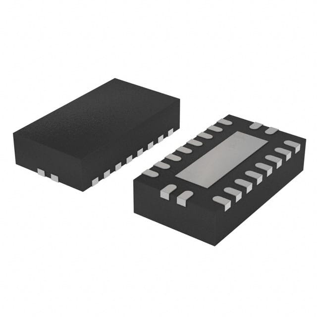
- Package: TSSOP-20
- Essence: This IC is designed to shift logic levels between different voltage domains, allowing seamless communication between devices operating at different voltage levels.
- Packaging/Quantity: Available in tape and reel packaging, with a quantity of 2500 units per reel.
Specifications
- Supply Voltage: 2.0V to 5.5V
- Input Voltage: -0.5V to VCC + 0.5V
- Output Voltage: -0.5V to VCC + 0.5V
- Operating Temperature Range: -40°C to +125°C
- Propagation Delay: 4.3ns (typical) at 5V supply voltage
- Output Drive Capability: ±24mA at 3.3V supply voltage
Detailed Pin Configuration
The 74VHCT541BQ,115 IC has a total of 20 pins arranged as follows:
+---+--+---+
   OE1 |1  +--+ 20| VCC
   A1  |2       19| A2
   B1  |3       18| B2
   GND |4       17| GND
   I1  |5       16| I2
   I3  |6       15| I4
   I5  |7       14| I6
   I7  |8       13| I8
   O1  |9       12| O2
   O3  |10      11| O4
       +----------+
Functional Features
- Octal buffer/line driver with 3-state outputs
- Inputs and outputs are compatible with both TTL and CMOS logic levels
- High-speed operation, suitable for applications requiring fast signal transmission
- Low power consumption, making it ideal for battery-powered devices
- Output drive capability allows direct interface with various loads
Advantages and Disadvantages
Advantages: - Wide supply voltage range enables compatibility with different systems - 3-state outputs provide flexibility in controlling signal flow - High-speed operation ensures efficient data transfer - Low power consumption extends battery life in portable devices
Disadvantages: - Limited output drive capability may not be suitable for driving heavy loads - Propagation delay may introduce timing issues in certain applications
Working Principles
The 74VHCT541BQ,115 is a logic level shifter that operates by receiving input signals from one voltage domain and shifting them to another voltage domain. It utilizes a combination of internal circuitry to ensure proper level shifting while maintaining signal integrity. The inputs and outputs are designed to be compatible with both TTL and CMOS logic levels, allowing seamless integration into various systems.
Detailed Application Field Plans
The 74VHCT541BQ,115 IC finds applications in a wide range of fields, including:
- Microcontroller-based systems
- Communication interfaces
- Data acquisition systems
- Industrial automation
- Consumer electronics
- Automotive electronics
- Medical devices
Its ability to shift logic levels between different voltage domains makes it an essential component in systems where intercommunication between devices operating at different voltage levels is required.
Detailed and Complete Alternative Models
Some alternative models that offer similar functionality to the 74VHCT541BQ,115 IC include:
- SN74LVC541A: Octal Buffer/Line Driver with 3-State Outputs
- MC74VHC541: Octal Buffer/Line Driver, Non-Inverting
- CD74HCT541: High-Speed CMOS Logic Octal Buffer/Line Driver
These alternative models can be considered based on specific application requirements and availability in the market.
Word count: 511 words
Sebutkan 10 pertanyaan dan jawaban umum terkait penerapan 74VHCT541BQ,115 dalam solusi teknis
Sure! Here are 10 common questions and answers related to the application of 74VHCT541BQ,115 in technical solutions:
Question: What is the function of the 74VHCT541BQ,115?
Answer: The 74VHCT541BQ,115 is an octal buffer/line driver with 3-state outputs.Question: What is the voltage supply range for this IC?
Answer: The voltage supply range for the 74VHCT541BQ,115 is typically between 4.5V and 5.5V.Question: How many inputs and outputs does this IC have?
Answer: The 74VHCT541BQ,115 has 8 inputs and 8 outputs.Question: Can I use this IC for level shifting applications?
Answer: Yes, the 74VHCT541BQ,115 can be used for level shifting as it supports both TTL and CMOS logic levels.Question: What is the maximum output current that this IC can drive?
Answer: The maximum output current for each channel of the 74VHCT541BQ,115 is typically around 8mA.Question: Is this IC compatible with other standard logic families?
Answer: Yes, the 74VHCT541BQ,115 is compatible with other standard logic families such as TTL and CMOS.Question: Can I connect multiple 74VHCT541BQ,115 ICs together?
Answer: Yes, you can connect multiple 74VHCT541BQ,115 ICs together to expand the number of inputs or outputs.Question: Does this IC have any built-in protection features?
Answer: The 74VHCT541BQ,115 has built-in ESD protection on all inputs and outputs.Question: What is the typical propagation delay of this IC?
Answer: The typical propagation delay for the 74VHCT541BQ,115 is around 6ns.Question: Can I use this IC in high-speed applications?
Answer: Yes, the 74VHCT541BQ,115 can be used in high-speed applications as it has a fast propagation delay and supports high-frequency operation.
Please note that the answers provided here are general and may vary depending on specific datasheet specifications and application requirements.