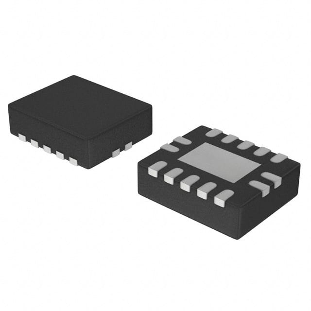
Encyclopedia Entry: 74VHC126BQ-Q100X
Product Overview
- Category: Integrated Circuit (IC)
- Use: Logic Gate Buffer/Driver
- Characteristics: High-Speed, Low-Power, Quad Bus Buffer with 3-State Outputs
- Package: BQFN (Quad Flat No-Lead) Package
- Essence: Buffering and driving signals in digital circuits
- Packaging/Quantity: Tape and Reel, 2500 units per reel
Specifications
- Supply Voltage Range: 2.0V to 5.5V
- Input Voltage Range: 0V to VCC
- Output Voltage Range: 0V to VCC
- Operating Temperature Range: -40°C to +125°C
- Propagation Delay Time: 4.5ns (typical)
- Output Current: ±8mA (maximum)
Detailed Pin Configuration
The 74VHC126BQ-Q100X IC has a total of 14 pins, which are assigned specific functions as follows:
- Pin 1: Output Enable (OE) - Active LOW enable input for all four buffers
- Pin 2: Input A1 - Input for buffer 1
- Pin 3: Output Y1 - Output for buffer 1
- Pin 4: GND - Ground reference
- Pin 5: Output Y2 - Output for buffer 2
- Pin 6: Input A2 - Input for buffer 2
- Pin 7: VCC - Positive power supply
- Pin 8: Output Y3 - Output for buffer 3
- Pin 9: Input A3 - Input for buffer 3
- Pin 10: Output Y4 - Output for buffer 4
- Pin 11: Input A4 - Input for buffer 4
- Pin 12: NC - No connection
- Pin 13: GND - Ground reference
- Pin 14: Output Enable (OE) - Active LOW enable input for all four buffers
Functional Features
- High-Speed Operation: The 74VHC126BQ-Q100X offers fast propagation delay times, making it suitable for high-speed digital circuits.
- Low Power Consumption: This IC is designed to operate at low power levels, reducing energy consumption in electronic systems.
- Quad Buffer with 3-State Outputs: It provides four independent buffer channels, each with a 3-state output, allowing multiple signal buffering and driving capabilities.
Advantages and Disadvantages
Advantages: - High-speed operation enables efficient signal buffering in fast digital circuits. - Low power consumption contributes to energy-efficient designs. - Quad buffer configuration allows for versatile signal buffering and driving applications.
Disadvantages: - Limited output current capacity may restrict its use in certain high-current applications. - The package size (BQFN) may require specialized equipment for soldering and handling.
Working Principles
The 74VHC126BQ-Q100X operates as a buffer/driver by receiving input signals and amplifying them to drive output loads. When the Output Enable (OE) pin is active LOW, the outputs are enabled and reflect the input signals. Conversely, when OE is inactive HIGH, the outputs enter a high-impedance state, effectively disconnecting them from the circuit.
Detailed Application Field Plans
The 74VHC126BQ-Q100X finds applications in various fields, including: 1. Microcontrollers and Digital Processors: Signal buffering between microcontrollers and peripheral devices. 2. Communication Systems: Buffering and driving signals in data transmission and reception circuits. 3. Industrial Automation: Interface buffering in control systems and PLCs. 4. Automotive Electronics: Signal conditioning and driving in automotive control modules. 5. Consumer Electronics: Buffering and driving signals in audio/video systems, gaming consoles, etc.
Detailed and Complete Alternative Models
- 74VHC125BQ-Q100X: Similar to 74VHC126BQ-Q100X but with tri-state outputs instead of 3-state outputs.
- 74AHC126BQ-Q100X: A variant with similar functionality but operates at a wider supply voltage range (2.0V to 6.0V).
- 74LVCH126BQ-Q100X: Low-voltage version with similar characteristics but designed for operation at 1.65V to 3.6V.
(Note: The above alternative models are just a few examples; there are several other alternatives available in the market.)
In conclusion, the 74VHC126BQ-Q100X is a high-speed, low-power quad bus buffer IC that finds applications in various digital circuits. Its versatile features, compact package, and availability of alternative models make it a popular choice among designers seeking efficient signal buffering and driving solutions.
Sebutkan 10 pertanyaan dan jawaban umum terkait penerapan 74VHC126BQ-Q100X dalam solusi teknis
Sure! Here are 10 common questions and answers related to the application of 74VHC126BQ-Q100X in technical solutions:
Question: What is the function of the 74VHC126BQ-Q100X?
Answer: The 74VHC126BQ-Q100X is a quad buffer/line driver with 3-state outputs.Question: What is the operating voltage range for this IC?
Answer: The operating voltage range for the 74VHC126BQ-Q100X is 2.0V to 5.5V.Question: How many buffers/line drivers are there in this IC?
Answer: The 74VHC126BQ-Q100X has four buffers/line drivers.Question: What is the maximum output current that each buffer can drive?
Answer: Each buffer in the 74VHC126BQ-Q100X can drive up to 8mA of current.Question: Can I use this IC for level shifting applications?
Answer: Yes, the 74VHC126BQ-Q100X can be used for level shifting between different voltage domains.Question: Is this IC suitable for high-speed applications?
Answer: Yes, the 74VHC126BQ-Q100X is designed for high-speed operation with propagation delays as low as 3.5ns.Question: Does this IC have built-in protection features?
Answer: Yes, the 74VHC126BQ-Q100X has built-in ESD protection on all inputs and outputs.Question: Can I connect the outputs of multiple 74VHC126BQ-Q100X ICs together?
Answer: Yes, the outputs of multiple ICs can be connected together without any additional components.Question: What is the temperature range for this IC?
Answer: The 74VHC126BQ-Q100X is designed to operate in the temperature range of -40°C to +125°C.Question: Are there any recommended decoupling capacitors for this IC?
Answer: It is recommended to place a 0.1µF decoupling capacitor between VCC and GND pins of each IC for stable operation.
Please note that these answers are general and may vary depending on the specific application and requirements.


