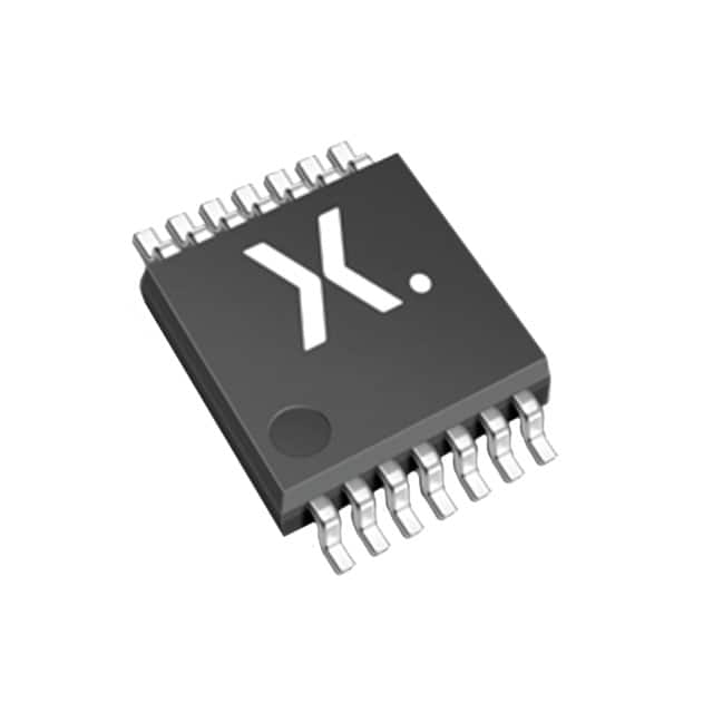
Lihat spesifikasi untuk detail produk.

74LVC86APW,112
Basic Information Overview
- Category: Integrated Circuit (IC)
- Use: Logic Gate
- Characteristics: Quad 2-input XOR gate
- Package: TSSOP-14
- Essence: High-speed CMOS technology
- Packaging/Quantity: Tape and reel, 2500 units per reel
Specifications
- Supply Voltage Range: 1.65V to 5.5V
- Input Voltage Range: 0V to VCC
- Output Voltage Range: 0V to VCC
- Operating Temperature Range: -40°C to +125°C
- Propagation Delay: 3.8ns (typical) at 3.3V supply voltage
Detailed Pin Configuration
The 74LVC86APW,112 has a TSSOP-14 package with the following pin configuration:
__    __
   A1 -| 1    14 |- VCC
   B1 -| 2    13 |- C1
   A2 -| 3    12 |- B2
   B2 -| 4    11 |- A2
   Y2 -| 5    10 |- B3
   Y1 -| 6     9 |- A3
  GND -| 7     8 |- Y3
       |_________|
Functional Features
- Quad 2-input XOR gate: The 74LVC86APW,112 consists of four independent XOR gates, each with two inputs and one output.
- High-speed operation: Utilizing high-speed CMOS technology, this IC provides fast switching times and low power consumption.
- Wide voltage range: It can operate within a wide supply voltage range from 1.65V to 5.5V, making it compatible with various systems.
- Low propagation delay: The typical propagation delay of 3.8ns ensures efficient signal processing.
Advantages and Disadvantages
Advantages: - High-speed operation allows for quick data processing. - Wide voltage range compatibility enhances versatility. - Low power consumption contributes to energy efficiency.
Disadvantages: - Limited number of XOR gates in a single package. - TSSOP-14 package may require careful handling during assembly.
Working Principles
The 74LVC86APW,112 is based on CMOS technology, which utilizes complementary pairs of MOS transistors to implement logic functions. In this case, the XOR gate performs an exclusive OR operation on its two input signals. The output is high (logic 1) only when the inputs differ, otherwise, it is low (logic 0).
Detailed Application Field Plans
The 74LVC86APW,112 can be used in various applications, including: 1. Digital communication systems 2. Data encryption and decryption circuits 3. Arithmetic logic units (ALUs) 4. Error detection and correction circuits 5. Signal processing systems
Detailed and Complete Alternative Models
Some alternative models that serve similar purposes are: - 74HC86: Similar quad 2-input XOR gate with a different package and voltage range. - CD4070: Quad 2-input XOR gate from another manufacturer. - SN74LS86: Quad 2-input XOR gate with different characteristics and package.
These alternatives provide options based on specific requirements such as voltage range, speed, and package type.
Word count: 314 words
Sebutkan 10 pertanyaan dan jawaban umum terkait penerapan 74LVC86APW,112 dalam solusi teknis
Sure! Here are 10 common questions and answers related to the application of 74LVC86APW,112 in technical solutions:
Q: What is the function of the 74LVC86APW,112? A: The 74LVC86APW,112 is a quad 2-input XOR gate integrated circuit (IC) that performs exclusive OR operations on two input signals.
Q: What is the operating voltage range for the 74LVC86APW,112? A: The 74LVC86APW,112 operates within a voltage range of 1.65V to 5.5V.
Q: What is the maximum output current of the 74LVC86APW,112? A: The maximum output current of the 74LVC86APW,112 is typically 32mA.
Q: Can the 74LVC86APW,112 be used in both digital and analog applications? A: No, the 74LVC86APW,112 is primarily designed for digital applications and may not be suitable for analog circuits.
Q: What is the propagation delay of the 74LVC86APW,112? A: The propagation delay of the 74LVC86APW,112 is typically around 4.3ns.
Q: Is the 74LVC86APW,112 compatible with other logic families? A: Yes, the 74LVC86APW,112 is compatible with various logic families such as TTL, CMOS, and LVTTL.
Q: Can the 74LVC86APW,112 handle high-speed data transmission? A: Yes, the 74LVC86APW,112 is designed to operate at high speeds and can handle fast data transmission.
Q: What is the power consumption of the 74LVC86APW,112? A: The power consumption of the 74LVC86APW,112 is relatively low, making it suitable for battery-powered applications.
Q: Can the 74LVC86APW,112 be used in automotive applications? A: Yes, the 74LVC86APW,112 is qualified for automotive applications and meets the necessary standards.
Q: Are there any specific precautions to consider when using the 74LVC86APW,112? A: It is important to follow the recommended operating conditions, such as voltage levels and temperature ranges, specified in the datasheet to ensure proper functionality and reliability of the IC.

