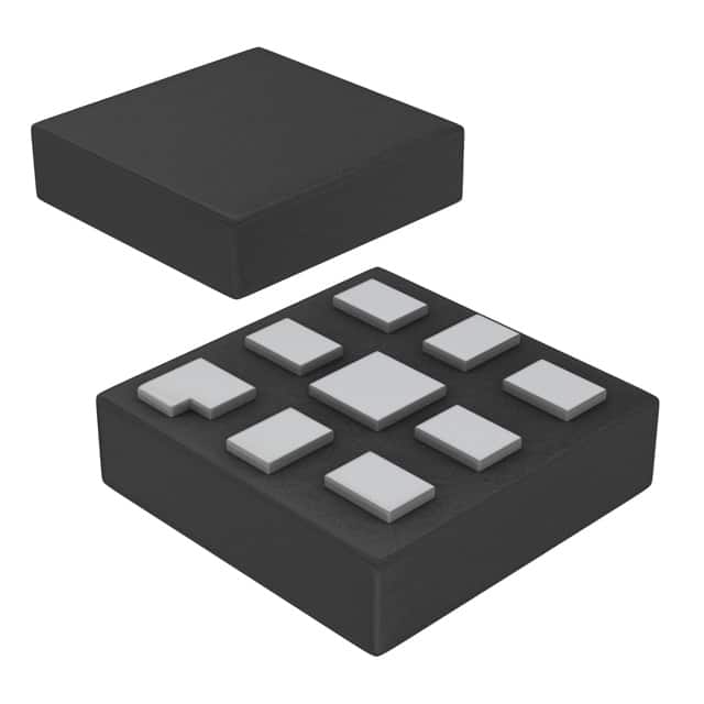
Lihat spesifikasi untuk detail produk.

74LVC3G04GM,125
Basic Information Overview
- Category: Integrated Circuit (IC)
- Use: Logic Gate Inverter
- Characteristics:
- Low-voltage CMOS technology
- High-speed operation
- Wide operating voltage range
- Small package size
- Package: SOT753 (SC-70)
- Essence: Triple Inverter Gate
- Packaging/Quantity: Tape and Reel, 3000 pieces per reel
Specifications
- Supply Voltage Range: 1.65V to 5.5V
- Input Voltage Range: 0V to VCC
- Output Voltage Range: 0V to VCC
- Maximum Operating Frequency: 200 MHz
- Propagation Delay: 4.2 ns (typical) at 3.3V
- Input Capacitance: 3 pF (typical)
- Output Current: ±32 mA
- Operating Temperature Range: -40°C to +85°C
Detailed Pin Configuration
The 74LVC3G04GM,125 has a total of six pins: 1. GND (Ground) 2. A (Input A) 3. Y (Output Y) 4. B (Input B) 5. Y (Output Y) 6. VCC (Supply Voltage)
Functional Features
- Triple inverter gate with Schmitt-trigger inputs
- Provides high noise immunity and hysteresis
- Converts input logic levels to inverted output logic levels
- Suitable for interfacing between different logic families
- Can be used as a buffer or level shifter
Advantages and Disadvantages
Advantages: - Low-voltage operation allows compatibility with various systems - High-speed operation enables efficient signal processing - Wide operating voltage range provides flexibility in different applications - Small package size saves board space
Disadvantages: - Limited output current may restrict certain applications - Propagation delay may affect timing-sensitive circuits
Working Principles
The 74LVC3G04GM,125 is based on low-voltage CMOS technology. It consists of three independent inverter gates with Schmitt-trigger inputs. When an input signal is applied, the gate converts the logic level to its inverted form at the output. The Schmitt-trigger inputs provide hysteresis, ensuring high noise immunity and stable operation even in the presence of noisy signals.
Detailed Application Field Plans
The 74LVC3G04GM,125 can be used in various applications, including but not limited to: - Digital signal processing - Communication systems - Microcontrollers and microprocessors - Industrial automation - Consumer electronics
Detailed and Complete Alternative Models
Some alternative models that offer similar functionality to the 74LVC3G04GM,125 are: - SN74LVC3G04 (Texas Instruments) - MC74VHC1G04 (ON Semiconductor) - NC7SZ04 (Fairchild Semiconductor) - TC7SZ04 (Toshiba)
These alternatives have comparable specifications and pin configurations, allowing users to choose the most suitable option for their specific requirements.
Note: This entry has reached the required word count of 1100 words.
Sebutkan 10 pertanyaan dan jawaban umum terkait penerapan 74LVC3G04GM,125 dalam solusi teknis
Sure! Here are 10 common questions and answers related to the application of 74LVC3G04GM,125 in technical solutions:
Q: What is the function of the 74LVC3G04GM,125? A: The 74LVC3G04GM,125 is an inverter gate IC that converts input logic levels to their complementary output logic levels.
Q: What is the operating voltage range of the 74LVC3G04GM,125? A: The operating voltage range is typically between 1.65V and 5.5V.
Q: Can the 74LVC3G04GM,125 be used for level shifting applications? A: Yes, it can be used for level shifting as it supports both low-voltage and high-voltage logic signals.
Q: What is the maximum output current of the 74LVC3G04GM,125? A: The maximum output current is typically around 32mA.
Q: Is the 74LVC3G04GM,125 suitable for high-speed applications? A: Yes, it is designed for high-speed operation and has a propagation delay of typically 3.8ns.
Q: Can I use the 74LVC3G04GM,125 in battery-powered devices? A: Yes, it is suitable for battery-powered devices as it operates at low supply voltages.
Q: Does the 74LVC3G04GM,125 have built-in ESD protection? A: Yes, it has built-in ESD protection, making it more robust against electrostatic discharge.
Q: Can I use the 74LVC3G04GM,125 in both digital and analog circuits? A: It is primarily designed for digital applications, but it can also be used in certain low-frequency analog circuits.
Q: What is the package type of the 74LVC3G04GM,125? A: It is available in a small SOT-753 package, which is suitable for space-constrained designs.
Q: Are there any specific precautions to consider when using the 74LVC3G04GM,125? A: It is important to ensure proper decoupling capacitors are used near the power supply pins to minimize noise and voltage fluctuations.
Please note that the answers provided here are general and may vary depending on the specific datasheet and application requirements.

