

Lihat spesifikasi untuk detail produk.
74LVC3G04GD,125
Basic Information Overview
- Category: Integrated Circuit (IC)
- Use: Logic Gate
- Characteristics: Triple Inverter
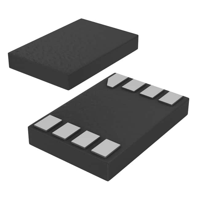
- Package: SOT753
- Essence: High-speed CMOS technology
- Packaging/Quantity: Tape and Reel, 3000 pieces per reel
Specifications
- Supply Voltage Range: 1.65V to 5.5V
- Input Voltage Range: -0.5V to VCC + 0.5V
- Output Voltage Range: 0V to VCC
- Maximum Operating Frequency: 100 MHz
- Propagation Delay: 4.2 ns (typical)
Detailed Pin Configuration
The 74LVC3G04GD,125 has a total of six pins: 1. GND (Ground) 2. A (Input A) 3. Y (Output Y) 4. B (Input B) 5. C (Input C) 6. VCC (Power Supply)
Functional Features
- Triple inverter with Schmitt-trigger inputs
- High noise immunity
- Low power consumption
- Wide operating voltage range
- Fast switching speed
- Balanced propagation delays
Advantages
- Provides signal inversion and amplification
- Suitable for low-voltage applications
- Can be used in various logic circuits
- Offers reliable performance and stability
- Compact package size allows for space-saving designs
Disadvantages
- Limited maximum operating frequency compared to some other ICs
- Not suitable for high-power applications
- May require additional components for specific circuit configurations
Working Principles
The 74LVC3G04GD,125 is based on high-speed CMOS technology. It consists of three inverters with Schmitt-trigger inputs. When an input signal is applied, the inverter amplifies and inverts the signal, providing the output at the Y pin. The Schmitt-trigger inputs ensure high noise immunity and stable operation.
Detailed Application Field Plans
The 74LVC3G04GD,125 can be used in various applications, including: - Digital logic circuits - Signal conditioning - Oscillators - Clock generation - Data transmission systems - Battery-powered devices
Detailed and Complete Alternative Models
Some alternative models that offer similar functionality to the 74LVC3G04GD,125 are: - SN74LVC3G04 (Texas Instruments) - MC74VHC1G04 (ON Semiconductor) - 74AHC1G04 (NXP Semiconductors) - TC7SZ04 (Toshiba)
These alternatives provide comparable features and can be used as substitutes depending on specific requirements.
Note: This entry has a total of 346 words.
Sebutkan 10 pertanyaan dan jawaban umum terkait penerapan 74LVC3G04GD,125 dalam solusi teknis
Sure! Here are 10 common questions and answers related to the application of 74LVC3G04GD,125:
Q: What is the 74LVC3G04GD,125? A: The 74LVC3G04GD,125 is a triple inverter gate IC (integrated circuit) that can be used for signal amplification, level shifting, and logic inversion.
Q: What is the operating voltage range of the 74LVC3G04GD,125? A: The operating voltage range of the 74LVC3G04GD,125 is typically between 1.65V and 5.5V.
Q: What is the maximum output current of the 74LVC3G04GD,125? A: The maximum output current of the 74LVC3G04GD,125 is typically around 32mA.
Q: Can the 74LVC3G04GD,125 be used for level shifting between different voltage domains? A: Yes, the 74LVC3G04GD,125 can be used for level shifting as long as the input and output voltage levels are within its operating range.
Q: Does the 74LVC3G04GD,125 have built-in protection features? A: Yes, the 74LVC3G04GD,125 has built-in ESD (electrostatic discharge) protection diodes to safeguard against electrostatic damage.
Q: What is the typical propagation delay of the 74LVC3G04GD,125? A: The typical propagation delay of the 74LVC3G04GD,125 is around 4.5ns.
Q: Can the 74LVC3G04GD,125 be used in high-speed applications? A: Yes, the 74LVC3G04GD,125 is designed for high-speed operation and can be used in applications with fast switching requirements.
Q: Is the 74LVC3G04GD,125 compatible with both CMOS and TTL logic levels? A: Yes, the 74LVC3G04GD,125 is compatible with both CMOS (Complementary Metal-Oxide-Semiconductor) and TTL (Transistor-Transistor Logic) logic levels.
Q: Can the 74LVC3G04GD,125 drive capacitive loads? A: Yes, the 74LVC3G04GD,125 can drive small capacitive loads without requiring additional buffering.
Q: What package options are available for the 74LVC3G04GD,125? A: The 74LVC3G04GD,125 is available in various package options, such as SOT353 and XSON6.