

Lihat spesifikasi untuk detail produk.
74LVC2G240DC-Q100H
Basic Information Overview
- Category: Integrated Circuit (IC)
- Use: Logic Gate Buffer/Driver
- Characteristics: Low-voltage, dual gate, non-inverting buffer/driver
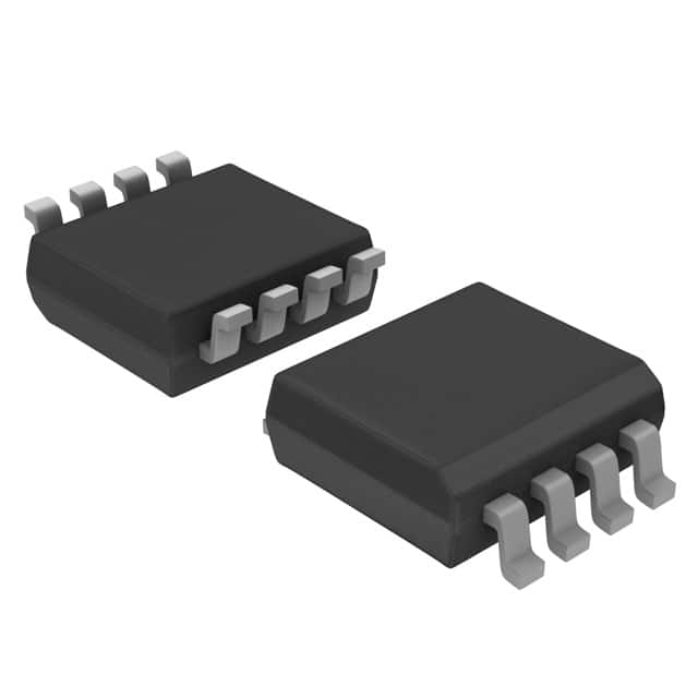
- Package: VSSOP (Very Small Outline Package)
- Essence: Provides voltage level shifting and signal amplification capabilities
- Packaging/Quantity: Tape and Reel, 3000 units per reel
Specifications
- Supply Voltage Range: 1.65V to 5.5V
- Input Voltage Range: -0.5V to VCC + 0.5V
- Output Voltage Range: 0V to VCC
- Maximum Operating Frequency: 80 MHz
- Number of Gates: 2
- Input/Output Type: CMOS
- High-Level Output Current: -32 mA
- Low-Level Output Current: 32 mA
- Propagation Delay: 4.3 ns (typical)
Detailed Pin Configuration
The 74LVC2G240DC-Q100H has a total of 8 pins arranged as follows:
___________
   A1 |           | VCC
   A2 |           | B1
   GND |           | B2
   OE  |           | Y1
   Y2  |           | GND
       -------------
Functional Features
- Dual non-inverting buffer/driver with 3-state outputs
- Provides voltage level shifting between different logic families
- Allows interfacing between low-voltage and higher-voltage systems
- Supports bidirectional communication
- Enables signal amplification and buffering for improved signal integrity
- 3-state output allows for bus sharing and multi-master systems
Advantages
- Wide supply voltage range allows compatibility with various systems
- Fast propagation delay ensures quick signal transmission
- Low power consumption for energy-efficient operation
- Small package size saves board space
- 3-state output enables flexible bus sharing
Disadvantages
- Limited number of gates (2) may not be sufficient for complex applications
- Not suitable for high-frequency applications due to limited maximum operating frequency
Working Principles
The 74LVC2G240DC-Q100H is a CMOS-based buffer/driver IC that operates as a voltage level shifter and signal amplifier. It consists of two non-inverting buffer/driver circuits with 3-state outputs. The inputs are compatible with both TTL and CMOS logic levels, allowing seamless interfacing between different logic families.
When the Output Enable (OE) pin is low, the outputs (Y1 and Y2) are active and reflect the input signals (A1 and A2). When OE is high, the outputs enter a high-impedance state, effectively disconnecting them from the bus and allowing other devices to drive the bus lines.
The IC operates within a wide supply voltage range, making it suitable for various low-voltage systems. It provides fast propagation delay, ensuring efficient signal transmission. Additionally, its low power consumption and small package size make it ideal for space-constrained applications.
Detailed Application Field Plans
The 74LVC2G240DC-Q100H finds applications in various fields, including: 1. Consumer electronics: Used in smartphones, tablets, and portable devices for voltage level shifting and signal buffering. 2. Automotive: Enables communication between low-voltage sensors and higher-voltage control units in automotive systems. 3. Industrial automation: Facilitates signal amplification and interfacing between different logic levels in industrial control systems. 4. Communication systems: Supports bidirectional communication and bus sharing in networking equipment and data transmission systems.
Detailed and Complete Alternative Models
- SN74LVC2G240DCUR: Similar dual buffer/driver IC with 3-state outputs, offered by Texas Instruments.
- MC74LVC2G240DTG: Dual non-inverting buffer/driver IC with 3-state outputs, manufactured by ON Semiconductor.
- NC7WZ240K8X: Ultra-small dual buffer/driver IC with 3-state outputs, produced by Fairchild Semiconductor.
(Note: The above alternative models are provided for reference and may have slight variations in specifications and package options.)
In conclusion, the 74LVC2G240DC-Q100H is a versatile logic gate buffer/driver IC that provides voltage level shifting, signal amplification, and buffering capabilities. Its wide supply voltage range, fast propagation delay, and small package size make it suitable for various applications in consumer electronics, automotive, industrial automation, and communication systems.
Sebutkan 10 pertanyaan dan jawaban umum terkait penerapan 74LVC2G240DC-Q100H dalam solusi teknis
Sure! Here are 10 common questions and answers related to the application of 74LVC2G240DC-Q100H in technical solutions:
Q: What is the 74LVC2G240DC-Q100H? A: The 74LVC2G240DC-Q100H is a dual non-inverting buffer/line driver IC with 3-state outputs.
Q: What is the operating voltage range of the 74LVC2G240DC-Q100H? A: The operating voltage range is from 1.65V to 5.5V.
Q: What is the maximum output current of the 74LVC2G240DC-Q100H? A: The maximum output current is typically 24mA.
Q: Can the 74LVC2G240DC-Q100H be used for level shifting between different voltage domains? A: Yes, it can be used for level shifting as long as the voltage levels are within its operating range.
Q: Does the 74LVC2G240DC-Q100H have built-in protection features? A: Yes, it has built-in protection against electrostatic discharge (ESD) and excessive power dissipation.
Q: What is the propagation delay of the 74LVC2G240DC-Q100H? A: The propagation delay is typically 4.3ns.
Q: Can the 74LVC2G240DC-Q100H drive capacitive loads? A: Yes, it can drive capacitive loads up to 50pF.
Q: Is the 74LVC2G240DC-Q100H suitable for high-speed applications? A: Yes, it is designed for high-speed operation and can be used in applications with fast switching requirements.
Q: Can the 74LVC2G240DC-Q100H be used in automotive applications? A: Yes, it is qualified for automotive applications and meets the AEC-Q100 standard.
Q: What package options are available for the 74LVC2G240DC-Q100H? A: The 74LVC2G240DC-Q100H is available in various package options, such as SOT353 and XSON8.