

Lihat spesifikasi untuk detail produk.
74LVC2G17GV-Q100H
Basic Information Overview
- Category: Integrated Circuit (IC)
- Use: Logic Gate Buffer/Driver
- Characteristics: High-speed, low-power, dual Schmitt-trigger buffer/driver
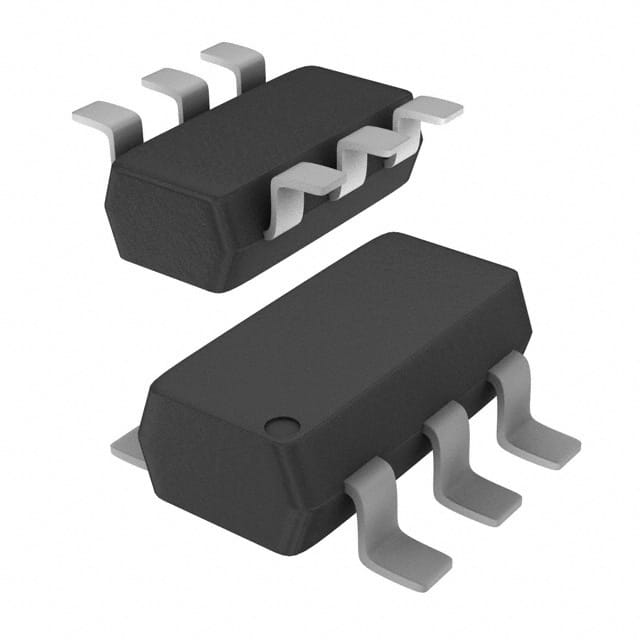
- Package: SOT753 (Thin Small Outline Transistor)
- Essence: Provides voltage level shifting and signal buffering capabilities
- Packaging/Quantity: Tape and Reel, 3000 pieces per reel
Specifications
- Supply Voltage Range: 1.65V to 5.5V
- High-Level Input Voltage: 0.7 x Vcc
- Low-Level Input Voltage: 0.3 x Vcc
- High-Level Output Voltage: 0.9 x Vcc
- Low-Level Output Voltage: 0.1 x Vcc
- Maximum Operating Frequency: 400 MHz
- Propagation Delay: 4.6 ns (typical)
Detailed Pin Configuration
The 74LVC2G17GV-Q100H has a total of 6 pins: 1. Pin 1: A Input (Schmitt-trigger) 2. Pin 2: Y Output 3. Pin 3: B Input (Schmitt-trigger) 4. Pin 4: GND (Ground) 5. Pin 5: Vcc (Supply Voltage) 6. Pin 6: Y Output
Functional Features
- Dual Schmitt-trigger buffer/driver with independent inputs and outputs
- Wide supply voltage range allows compatibility with various systems
- High-speed operation enables efficient signal processing
- Low power consumption for energy-efficient applications
- Schmitt-trigger inputs provide hysteresis, improving noise immunity
Advantages
- Compact package size saves board space
- Wide supply voltage range enhances versatility
- High-speed operation facilitates rapid data transmission
- Low power consumption prolongs battery life in portable devices
- Schmitt-trigger inputs ensure reliable signal processing in noisy environments
Disadvantages
- Limited number of input/output channels (dual)
- Propagation delay may affect timing-sensitive applications
- Sensitive to electrostatic discharge (ESD) and voltage spikes
Working Principles
The 74LVC2G17GV-Q100H operates as a buffer/driver, receiving digital signals at its input pins (A and B) and providing amplified and level-shifted signals at the output pins (Y). The Schmitt-trigger inputs allow for noise-immune signal detection by introducing hysteresis. The IC's internal circuitry ensures high-speed operation while consuming minimal power.
Detailed Application Field Plans
The 74LVC2G17GV-Q100H is commonly used in various electronic systems that require voltage level shifting and signal buffering. Some application fields include: 1. Communication Systems: Signal amplification and level shifting in data transmission circuits. 2. Industrial Automation: Interface between different logic families or voltage domains. 3. Automotive Electronics: Buffering and level shifting in automotive control units. 4. Consumer Electronics: Signal conditioning in audio/video equipment, smartphones, and tablets. 5. IoT Devices: Voltage level translation in sensor networks and smart home automation.
Detailed and Complete Alternative Models
- SN74LVC2G17DBVR - Texas Instruments
- MC74VHC1G17DFT1G - ON Semiconductor
- TC7SZ17FU - Toshiba
- NC7SZ17P5X - Fairchild Semiconductor
- NCV8170DR2G - ON Semiconductor
(Note: This list is not exhaustive and other alternative models from different manufacturers are available.)
This entry provides an overview of the 74LVC2G17GV-Q100H integrated circuit, including its basic information, specifications, pin configuration, functional features, advantages, disadvantages, working principles, application field plans, and alternative models.
Sebutkan 10 pertanyaan dan jawaban umum terkait penerapan 74LVC2G17GV-Q100H dalam solusi teknis
Sure! Here are 10 common questions and answers related to the application of 74LVC2G17GV-Q100H in technical solutions:
Q: What is the 74LVC2G17GV-Q100H? A: The 74LVC2G17GV-Q100H is a dual Schmitt-trigger buffer with open-drain outputs, designed for low-voltage applications.
Q: What is the voltage range supported by the 74LVC2G17GV-Q100H? A: The 74LVC2G17GV-Q100H supports a wide voltage range from 1.65V to 5.5V.
Q: What is the maximum output current of the 74LVC2G17GV-Q100H? A: The maximum output current of the 74LVC2G17GV-Q100H is typically 32mA.
Q: Can the 74LVC2G17GV-Q100H be used in high-speed applications? A: Yes, the 74LVC2G17GV-Q100H is designed for high-speed operation, making it suitable for various applications.
Q: Does the 74LVC2G17GV-Q100H have built-in protection features? A: Yes, the 74LVC2G17GV-Q100H has built-in ESD protection, which helps safeguard against electrostatic discharge.
Q: How many inputs does the 74LVC2G17GV-Q100H have? A: The 74LVC2G17GV-Q100H has two inputs, labeled A and B.
Q: Can the 74LVC2G17GV-Q100H be used as a level shifter? A: Yes, the 74LVC2G17GV-Q100H can be used as a level shifter to convert signals between different voltage levels.
Q: What is the typical propagation delay of the 74LVC2G17GV-Q100H? A: The typical propagation delay of the 74LVC2G17GV-Q100H is around 4.5ns.
Q: Is the 74LVC2G17GV-Q100H available in different package options? A: Yes, the 74LVC2G17GV-Q100H is available in various package options, such as SOT353 and XSON6.
Q: Can the 74LVC2G17GV-Q100H be used in automotive applications? A: Yes, the 74LVC2G17GV-Q100H is qualified for automotive applications and meets the necessary standards.
Please note that these answers are general and may vary depending on specific datasheet specifications and application requirements.